Credit: Jang-sik Lee(POSTECH)
Netflix, which provides an online streaming service around the world, has 42 million videos and about 160 million subscribers in total. It takes just a few seconds to download a 30-minute video clip and you can watch a show within 15 minutes after it airs. As distribution and transmission of high-quality contents are growing rapidly, it is critical to develop reliable and stable semiconductor memories.
To this end, POSTECH research team has developed a memory device using a two-dimensional layered-structure material, unlocking the possibility of commercializing the next-generation memory device that can be stably operated at a low power.
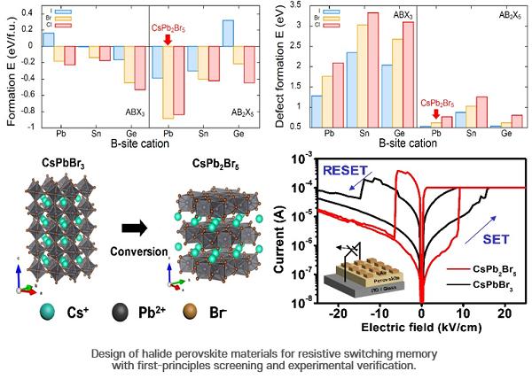
POSTECH research team consisting of Professor Jang-Sik Lee of the Department of Materials Science and Engineering, Professor Donghwa Lee of the Division of Advanced Materials Science, Youngjun Park, and Seong Hun Kim in the PhD course succeeded in designing an optimal halide perovskite material (CsPb2Br5) that can be applied to a ReRAM*1 device by applying the first-principles calculation*2 based on quantum mechanics. The findings were published in Advanced Science.
The ideal next-generation memory device should process information at high speeds, store large amounts of information with non-volatile characteristics where the information does not disappear when power is off, and operate at low power for mobile devices.
The recent discovery of the resistive switching property in halide perovskite materials has led to worldwide active research to apply them to ReRAM devices. However, the poor stability of halide perovskite materials when they are exposed to the atmosphere have been raised as an issue.
The research team compared the relative stability and properties of halide perovskites with various structures using the first principles calculation2. DFT calculations predicted that CsPb2Br5, a two-dimensional layered structure in the form of AB2X5, may have better stability than the three-dimensional structure of ABX3 or other structures (A3B2X7, A2BX4), and that this structure could show improved performance in memory devices.
To verify this result, CsPb2Br5, an inorganic perovskite material with a two-dimensional layered structure, was synthesized and applied to memory devices for the first time. The memory devices with a three-dimensional structure of CsPbBr3 lost their memory characteristics at temperatures higher than 100 °C. However, the memory devices using a two-dimensional layered-structure of CsPb2Br5 maintained their memory characteristics over 140 °C and could be operated at voltages lower than 1V.
Professor Jang-Sik Lee who led the research commented, “Using this materials-designing technique based on the first-principles screening and experimental verification, the development of memory devices can be accelerated by reducing the time spent on searching for new materials. By designing an optimal new material for memory devices through computer calculations and applying it to actually producing them, the material can be applied to memory devices of various electronic devices such as mobile devices that require low power consumption or servers that require reliable operation. This is expected to accelerate the commercialization of next-generation data storage devices.”
###
This research was conducted with the support from the Future Materials Discovery Project and the Mid-career Researcher Program of the Ministry of Science and ICT and the National Research Foundation of Korea.
Media Contact
Jinyoung Huh
[email protected]
Original Source
http://www.
Related Journal Article
http://dx.


