Credit: by Qingyang Bao, Weijia Li, Peizhen Xu, Ming Zhang, Daoxin Dai, Pan Wang, Xin Guo, and Limin Tong
In the past decade, on-chip nanophotonics has attracted increasing attention for the realization of integrated photonic circuits with faster operation, broader bandwidth, lower power consumption and higher compactness. While a number of on-chip nanophotonic devices and circuits have been successfully fabricated using a complementary metal-oxide semiconductor (CMOS) -compatible technique, on-chip light sources remain challenging. On the other hand, bottom-up grown semiconductor nanowires have long been used for nanoscale waveguide lasers. In recent years, increasing attention has been paid to the integration of active nanowires with on-chip planar waveguides for on-chip light sources. However, due to the large discrepancy in fabrication techniques, refractive index and geometric compatibility between a freestanding nanowire and an on-chip planar waveguide, a variety of issues, including a relatively low coupling efficiency, ineffective mode selection and low reproductivity, have yet to be addressed.
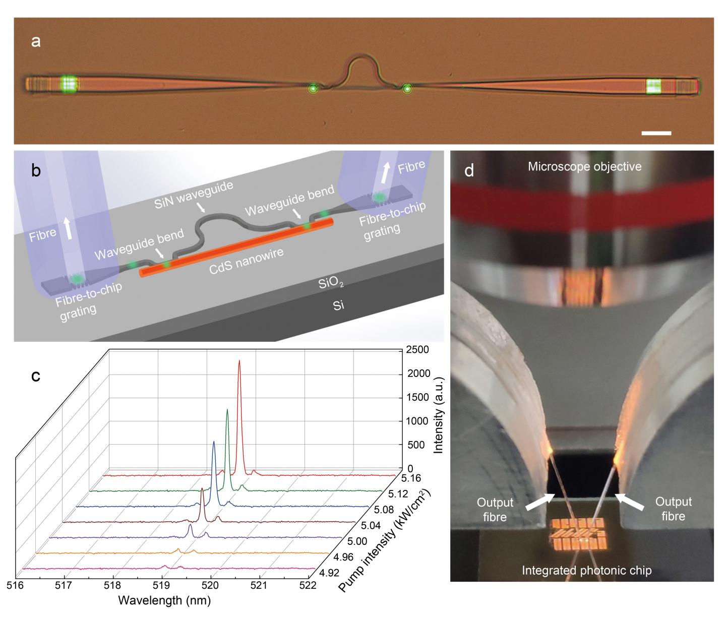
In a new paper published in Light Science & Application, scientists from the State Key Laboratory of Modern Optical Instrumentation, College of Optical Science and Engineering, Zhejiang University, China demonstrated an on-chip single-mode CdS nanowire laser with high coupling efficiency. The mode selection is realized using a Mach-Zehnder interferometer (MZI) structure. When the pumping intensity exceeds the lasing threshold of 4.9 kW/cm2, on-chip single-mode lasing at approximately 518.9 nm is achieved with a linewidth of 0.1 nm and a side-mode suppression ratio of 20 (13 dB). The output of the nanowire laser is channelled into an on-chip SiN waveguide with high efficiency (up to 58%) by evanescent coupling, and the directional coupling ratio between the two output ports can be varied from 90% to 10% by predesigning the coupling length of the SiN waveguide. Benefitting from the great diversity of the available nanowire materials and high flexibility for bandgap engineering, the on-chip integration scheme demonstrated here can be readily extended to realize on-chip nanolasers from the ultraviolet to near-infrared ranges, which may offer new opportunities for both semiconductor nanowires and on-chip photonic devices.
These scientists summarize the fabrication and operational principle of the laser:
“We use micromanipulation under an optical microscope to integrate a CdS nanowire onto a SiN chip and form a hybrid MZI structure with excellent reproducibility. By using the MZI for mode selection, we operate the laser in single mode. We can also change the output ratios between the two ports of the lasing MZI by using different coupling lengths of the waveguide bends.”
“The overall size of the hybrid MZI structure is kept below 100 μm. Fibre-to-chip grating couplers are designed at both ends of the SiN waveguide, which couple the laser signal from the on-chip SiN waveguide into standard optical fibres for optical characterization.” “By comparing the lasing output intensities from the nanowire end and the grating area, we estimate the fractional power channelled into the SiN waveguide to be approximately 58%, much higher than previous results obtained in chip integrated nanowire lasers, and can be further improved by optimizing the coupling efficiency between the nanowire and the SiN waveguide.” they added.
“Benefitting from the great diversity of the available nanowire materials and high flexibility for bandgap engineering, the on-chip integration scheme demonstrated here can be readily extended to realize on-chip nanolasers from the ultraviolet to near-infrared ranges, and the on-chip single-mode nanowire laser may thus offer an opportunity to develop on-chip physical and biochemical optical sensors with higher stability and compactness. ” the scientists forecast.
###
Media Contact
Xin Guo
[email protected]
Related Journal Article
http://dx.


