Credit: MRI/Penn State
To further shrink electronic devices and to lower energy consumption, the semiconductor industry is interested in using 2D materials, but manufacturers need a quick and accurate method for detecting defects in these materials to determine if the material is suitable for device manufacture. Now a team of researchers has developed a technique to quickly and sensitively characterize defects in 2D materials.
Two-dimensional materials are atomically thin, the most well-known being graphene, a single-atom-thick layer of carbon atoms.
“People have struggled to make these 2D materials without defects,” said Mauricio Terrones, Verne M. Willaman Professor of Physics, Penn State. “That’s the ultimate goal. We want to have a 2D material on a four-inch wafer with at least an acceptable number of defects, but you want to evaluate it in a quick way.”
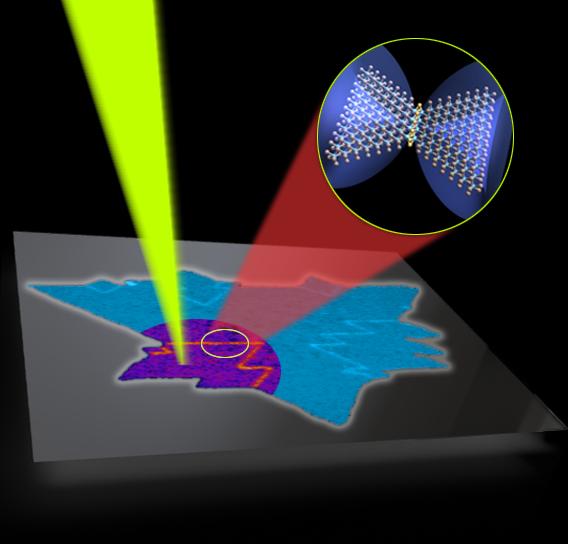
The researchers’ — who represent Penn State, Northeastern University, Rice University and Universidade Federal de Minas Gerais in Brazil – solution is to use laser light combined with second harmonic generation, a phenomenon in which the frequency of the light shone on the material reflects at double the original frequency. They add dark field imaging, a technique in which extraneous light is filtered out so that defects shine through. According to the researchers, this is the first instance in which dark field imaging was used, and it provides three times the brightness of the standard bright field imaging method, making it possible to see types of defects previously invisible.
“The localization and identification of defects with the commonly used bright field second harmonic generation is limited because of interference effects between different grains of 2D materials,” said Leandro Mallard, a senior author on a recent paper in Nano Letters and a professor at Universidade Federal de Minas Gerais. “In this work we have shown that by the use of dark field SHG we remove the interference effects and reveal the grain boundaries and edges of semiconducting 2D materials. Such a novel technique has good spatial resolution and can image large area samples that could be used to monitor the quality of the material produced in industrial scales.”
Vincent H. Crespi, Distinguished Professor of Physics, Materials Science and Engineering, and Chemistry, Penn State, added, “Crystals are made of atoms, and so the defects within crystals — where atoms are misplaced — are also of atomic size.
“Usually, powerful, expensive and slow experimental probes that do microscopy using beams of electrons are needed to discern such fine details in a material,” said Crespi. “Here, we use a fast and accessible optical method that pulls out just the signal that originates from the defect itself to rapidly and reliably find out how 2D materials are stitched together out of grains oriented in different ways.”
Another coauthor compared the technique to finding a particular zero on a page full of zeroes.
“In the dark field, all the zeroes are made invisible so that only the defective zero stands out,” said Yuanxi Wang, assistant research professor at Penn State’s Materials Research Institute.
The semiconductor industry wants to have the ability to check for defects on the production line, but 2D materials will likely be used in sensors before they are used in electronics, according to Terrones. Because 2D materials are flexible and can be incorporated into very small spaces, they are good candidates for multiple sensors in a smartwatch or smartphone and the myriad of other places where small, flexible sensors are required.
“The next step would be an improvement of the experimental setup to map zero dimension defects — atomic vacancies for instance — and also extend it to other 2D materials that host different electronic and structural properties,” said lead author Bruno Carvalho, a former visiting scholar in Terrones’ group,
###
Other co-authors on the Nano Letters paper, titled “Nonlinear Dark-Field Imaging of One-Dimensional Defects in Monolayer Dichalcogenides,” are Kuzanori Fujisawa, Tianyi Zhang, Ethan Kahn, Ismail Bilgin, Pulickel Ajayan, Ana de Paula, Marcos Pimenta and Swastik Kar.
The National Science Foundation, The Air Force Office of Scientific Research and various Brazilian funding agencies funded this work.
Media Contact
A’ndrea Elyse Messer
[email protected]
814-865-5689
Related Journal Article
http://dx.


