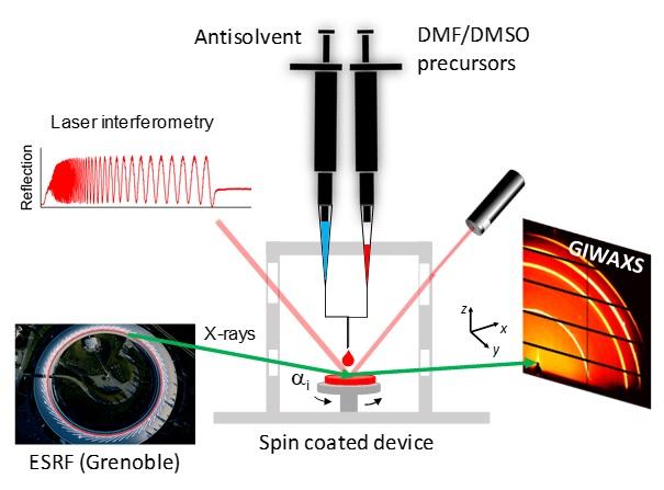
Credit: G. Portale, University of Groningen
Lead-based perovskites are very promising materials for the production of solar panels. They efficiently turn light into electricity but they also present some major drawbacks: the most efficient materials are not very stable, while lead is a toxic element. University of Groningen scientists are studying alternatives to lead-based perovskites. Two factors that significantly affect the efficiency of these solar cells are the ability to form thin films and the structure of the materials in the solar cells. Therefore, it is very important to investigate in situ how lead-free perovskite crystals form and how the crystal structure affects the functioning of the solar cells. The results of the study were published in the journal Advanced Functional Materials on 31 March.
Photovoltaic cells that are based on hybrid perovskites were first introduced in 2009 and rapidly became almost as efficient as standard silicon solar cells. These materials have a very distinctive crystal structure, known as the perovskite structure. In an idealized cubic unit cell, anions form an octahedron around a central cation, while the corners of the cube are occupied by other, larger cations. Different ions can be used to create different perovskites.
Spin coating
The best results in solar cells have been obtained using perovskites with lead as the central cation. As this metal is toxic, tin-based alternatives have been developed, for example, formamidinium tin iodide (FASnI3). This is a promising material; however, it lacks the stability of some of the lead-based materials. Attempts have been made to mix the 3D FASnI3 crystals with layered materials, containing the organic cation phenylethylammonium (PEA). ‘My colleague, Professor Maria Loi, and her research team showed that adding a small amount of this PEA produces a more stable and efficient material,’ says Assistant Professor Giuseppe Portale. ‘However, adding a lot of it reduces the photovoltaic efficiency.’
That is where Portale comes in. Perovskites have been studied for a long time by Professor of Photophysics and Optoelectronics Maria Loi, while Portale developed an X-ray diffraction technique that allows him to study the rapid formation of thin films in real-time during spin-coating from solution. On a laboratory scale, the perovskite films are generally made by spin coating, a process in which a precursor solution is delivered onto a fast-spinning substrate. Crystals grow as the solvent evaporates. At the beamline BM26B-DUBBLE at the European Synchrotron Radiation Facility (ESRF) in Grenoble, France, Portale investigated what happens during the tin-perovskite film formation.
Interface
‘Our initial idea, which was based on ex situ investigations, was that the oriented crystals grow from the substrate surface upwards,’ Portale explains. However, the in situ results showed the opposite: crystals start to grow at the air/solution interface. During his experiments, he used 3D FASnI3 with the addition of different amounts of the 2D PEASnI4. In the pure 3D perovskite, crystals started to form at the surface but also in the bulk of the solution. However, adding a small amount of the 2D material suppressed bulk crystallization and the crystals only grew from the interface.
‘PEA molecules play an active role in the precursor solution of the perovskites, stabilizing the growth of oriented 3D-like crystals through coordination at the crystal’s edges. Moreover, PEA molecules prevent nucleation in the bulk phase, so crystal growth only takes place at the air/solvent interface,’ Portale explains. The resulting films are composed of aligned 3D-like perovskite crystals and a minimal amount of 2D-like perovskite, located at the bottom of the film. The addition of low concentrations of the 2D material produces a stable and efficient photovoltaic material, while the efficiency drops dramatically at high concentrations of this 2D material.
Insulator
The experiments by Portale and Loi can explain this observation: ‘The 2D-like perovskite is located at the substrate/film interface. Increasing the content of the 2D material to above a certain amount causes the formation of an extended 2D-like organic layer that acts as an insulator, with detrimental effect for the device’s efficiency.’ The conclusion of the study is that the formation of this insulating layer must be prevented to achieve a highly efficient and stable tin-based perovskite. ‘The next step is to realize this, for example by playing with solvents, temperature or specific perovskite/substrate interactions that can break up the formation of this thick insulating layer.’
Simple Science Summary
Just over ten years ago, scientists discovered a new, promising material that could convert light into electricity: metal-halide perovskite. The first solar cell perovskites contained lead, which is toxic. Soon, perovskites were developed that were based on tin, but these were not very stable. A few years ago, scientists at the University of Groningen demonstrated that adding another type of perovskite – one that forms two-dimensional layers instead of three-dimensional crystals – increased the stability; however, it reduced efficiency. University of Groningen scientists have now ‘watched’ how thin films of tin-based perovskite crystals grow. They discovered that in mixtures of 3D and 2D perovskites, the 2D component helps to orient the 3D-like crystals but, at the same time, the 2D perovskite forms an insulating layer that is in contact with the substrate. By breaking up this insulating layer, it should be possible to create more efficient and stable tin-based perovskite solar panels.
###
Reference: Jingjin Dong, Shuyan Shao, Simon Kahmann, Alexander J. Rommens, Daniel Hermida?Merino, Gert H. ten Brink, Maria A. Loi & Giuseppe Portale: Mechanism of Crystal Formation in Ruddlesden-Popper Sn?Based Perovskites. Advanced Functional Materials, 31 March 2020
Media Contact
Rene Fransen
[email protected]
Original Source
https:/
Related Journal Article
http://dx.


