Credit: Junichi Yamaguchi, Yasunobu Sugimoto, Shintaro Sato, Hiroko Yamada
With literally the thickness of one carbon atom and electrical properties that can surpass those of standard semiconductor technologies, graphene nanoribbons promise a new generation of miniaturized electronic devices. The theory, however, remains far ahead of reality, with current graphene nanoribbons falling short of their potential. A new collaborative study seen in Communications Materials by a project of CREST, JST Japan including Nara Institute of Science and Technology (NAIST), Fujitsu Laboratories Ltd. and Fujitsu Ltd., and the University of Tokyo reports the first ever 17-carbon wide graphene nanoribbon and confirms it has the smallest bandgap seen to date among known graphene nanoribbons prepared by a bottom-up manner.
Large-scale integrated circuits (LSIs) that use silicon semiconductors are used in a wide range of electronic devices, anywhere from computers to smartphones. They are actually supporting our lives and almost everything else these days. However, although LSIs have improved device performance by reducing the size of the devices, LSI miniaturization is approaching its limit. At the same time, commercial demand continues to put pressure on companies to make higher performing smartphones at smaller sizes, while industry pressure is demanding large-scale manufacturing with smaller equipment.
Other methods and/or materials are definitely needed to solve these problems, says the group leader Dr. Shintaro Sato, Fujitsu Ltd.
“Silicon semiconductors are giving us better performance at smaller sizes. However, we are reaching the limit in how small we can make devices. Thus, we have high expectations for the performance of graphene nanoribbons, which have semi-conducting properties that are only one atom thick – a 2D material,” he notes.
Graphene nanoribbons are honeycomb-like structures and, compared to graphene and carbon nanotubes, are the lesser known carbon-based semiconductor family member. Graphene nanoribbons exhibit unique electronic and magnetic properties that do not appear in two-dimensional graphene.
“Interestingly, the electronic and magnetic properties of graphene nanoribbons are widely tuned as a function of the width and edge structure.” says Prof. Hiroko Yamada at NAIST.
Armchair-type graphene nanoribbons, which are promising type of nanoribbon for device application, display width-dependent band gap. They can be classified into three subfamilies (3p, 3p + 1, 3p + 2), their band gaps being inversely proportional to the width of those families. Basically, wider armchair-edge graphene nanoribbons belonging to the 3p + 2 subfamily have the smallest bandgaps among different graphene nanoribbons, having considerable potential to be exploited in GNR-based devices.
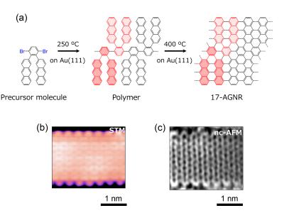
So far, 13-armchair graphene nanoribbons belonging to the 3p + 1 subfamily with a band gap of more than 1 eV have been reported, but Sato, Yamada and colleagues show the synthesis of a 17-graphene nanoribbon belonging to the 3p + 2 subfamily, which have even smaller bandgaps.
The graphene nanoribbon synthesis was based on the bottom-up approach, called “on-surface synthesis,” and a dibromobenzene-based molecule was used as a precursor for on-surface graphene nanoribbon synthesis.
“There are many methods to synthesize graphene nanoribbons, but to produce atomically precise graphene nanoribbons, we decided to use the bottom-up approach. The important point is that the structure of the precursor can define the ultimate structure of graphene nanoribbons if we use the bottom-up approach,” explains NAIST’s Dr. Hironobu Hayashi, who also contributed to the study.
Scanning tunnel microscopy and spectroscopy by Dr. Junichi Yamaguchi at Fujitsu. Ltd. and non-contact atomic force microscopy by Dr. Akitoshi Shiotari and Prof. Yoshiaki Sugimoto at The University of Tokyo confirmed the atomic and electronic structure of the acquired 17-armchair graphene nanoribbons. Additionally, the experimentally obtained bandgap of 17-armchair graphene nanoribbons was found to be 0.6 eV, and this is the first demonstration of the synthesis of graphene nanoribbons having a band gap smaller than 1 eV in a controlled manner.
“We expect these 17-carbon wide graphene nanoribbons to pave the way for new GNR-based electronic devices,” says Sato.
###
Resource
Title: Small bandgap features achieved in atomically precise 17-atom-wide armchair-edged graphene nanoribbons
Authors: Junichi Yamaguchi, Hironobu Hayashi, Hideyuki Jippo, Akitoshi Shiotari, Manabu Ohtomo, Mitsuhiro Sakakura, Nao Hieda, Naoki Aratani, Mari Ohfuchi, Yoshiaki Sugimoto, Hiroko Yamada & Shintaro Sato
Journal: Communications Materials
DOI: 10.1038/s43246-020-0039-9
Information about Prof. Yamada lab can be found at the following website:
https:/
Media Contact
Takahito Shikano
[email protected]
Related Journal Article
http://dx.


