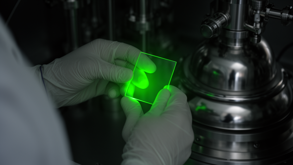
Perovskite light-emitting diodes have long been celebrated as one of the most exciting frontiers in display and lighting technology, promising vivid colors and high efficiency at potentially very low cost. Yet almost all of the headline-grabbing devices reported so far have been made by solution processing, in which the light-emitting layer is coated from an ink. That approach works beautifully in the laboratory, but it sits awkwardly with the way commercial displays and lighting panels are actually manufactured, where vacuum deposition dominates because it produces exquisitely uniform films over large areas. A new study published in Communications Engineering by Dian Luo, Shun-Wei Liu and their colleagues at Ming Chi University of Technology and partner institutions in Taiwan now shows that the vacuum route, long considered the poor relation of perovskite optoelectronics, can deliver green emitters that are both highly efficient and spectrally pure, provided one crucial ingredient is added to tame the way the crystals grow.
The team’s starting point was a co-evaporated emissive layer built from cesium bromide and lead bromide, the inorganic backbone of an all-inorganic cesium lead bromide perovskite. Evaporating these two compounds in a vacuum chamber sidesteps the solvents, annealing steps and batch-to-batch variability that plague solution methods, and it means the perovskite layer can be deposited directly on top of the organic charge-transport layers that are standard in OLED fabrication. The problem is that vacuum-deposited perovskites crystallize in an uncontrolled fashion: as the material condenses on the cold substrate, grains grow to wildly different sizes, the local chemical coordination around lead atoms varies from place to place, and a dense population of defects forms. Those defects act as traps that capture charge carriers and dissipate their energy as heat rather than light, a process known as trap-assisted nonradiative recombination, and it is the single biggest reason vacuum-processed perovskite LEDs have lagged behind their solution-processed cousins.
The Taiwanese researchers’ solution is elegantly simple. They introduced phenethylammonium bromide, a bulky organic ammonium salt, into the vacuum co-evaporation process alongside the cesium bromide and lead bromide. Because the compound sublimes, it can be delivered through the gas phase just like the inorganic components, which means the entire emissive stack remains fully compatible with the vacuum deposition lines used in industry. In solution-processed perovskites, bulky ammonium additives are routinely used to passivate surfaces and form low-dimensional phases, but incorporating them into a vacuum process had remained a stubborn challenge. Here, the phenethylammonium bromide acts as a crystallization regulator: it moderates the rate at which the perovskite grains grow, prevents any single grain from ballooning excessively at the expense of its neighbors, and reshapes the local coordination environment around the lead bromide framework so that fewer defective sites are created in the first place.
The consequences of this phase engineering show up clearly in the film quality. With the additive present, the emissive layer becomes markedly more uniform, with a more even grain-size distribution and a reduced density of trap states. Fewer traps mean that a larger fraction of the electrons and holes injected into the device recombine radiatively, emitting photons of green light instead of losing their energy silently. In LED terminology, the radiative efficiency of the emissive layer rises, and that improvement flows directly into the device figures of merit. The researchers report that their optimized devices reach a maximum external quantum efficiency of 10.2 percent, meaning that just over one in ten of the electrical charges pushed into the diode emerges as a usable photon leaving the device. For a vacuum-deposited green perovskite LED, that is a significant milestone, achieved without any of the solvent engineering tricks available to solution processors.
The other performance numbers are equally striking. The devices deliver a current efficiency of 36.5 candelas per ampere and a power efficiency of 35.8 lumens per watt, figures that indicate the diodes convert electrical power into visible green light with respectable economy. They can also be driven hard: the team measured luminance exceeding 12,600 candelas per square meter, a brightness level comfortably above what is needed for high-peak-brightness display applications such as HDR content or outdoor panels. Perhaps most importantly for anyone imagining these devices in a commercial product, the emission is not just bright but clean. The spectrum peaks at 518 nanometers, squarely in the green, with a full width at half maximum of only 20 nanometers. That narrow linewidth is a hallmark of perovskite emitters and one of their key advantages over conventional organic OLED emitters, whose broader spectra must be filtered to hit the wide-gamut color standards used in modern displays.
Spectral stability is where many emissive materials stumble, and it is an area where this work makes a particularly convincing case. Some LED technologies shift their emission color as the drive voltage or current changes, which is disastrous for a display, because a pixel that turns from green toward yellow as brightness increases destroys color accuracy. The researchers demonstrated that their devices remain spectrally stable under varying drive conditions, with the 518-nanometer peak holding its position and its 20-nanometer width. This stability suggests that the phase engineering has produced a genuinely robust emissive environment, one in which the perovskite does not undergo field-driven changes in its structure or its dimensionality when the device is pushed to different operating points. It is exactly the kind of behavior a display engineer needs to trust a new emitter chemistry.
Operational lifetime remains the honest caveat in the story. The team measured an operational lifetime of 4,388 seconds, roughly 73 minutes, at an initial luminance of 500 candelas per square meter. That is a meaningful benchmark figure for an early-stage vacuum-deposited perovskite LED and a solid baseline for future optimization, but it is still far from the tens of thousands of hours that commercial displays demand. The same defect chemistry that limits efficiency also drives degradation, so the additive strategy that suppresses traps may ultimately help longevity as well, but extending lifetime will require further work on encapsulation, electrode engineering and the stability of the perovskite lattice itself. The authors note that the study was supported by the National Science and Technology Council of Taiwan along with university funding, reflecting a sustained national investment in perovskite and organic electronics research.
What makes this result resonate beyond the laboratory is its manufacturing message. The entire emissive layer was produced by co-evaporation in a vacuum chamber, and the corresponding author has acknowledged the contribution of an industry engineer from Syskey Technology in Taiwan who helped design the perovskite fabrication chambers, underscoring that the work was done with real deposition hardware rather than laboratory-scale improvisation. Because vacuum deposition is already the backbone of OLED manufacturing, a perovskite emitter that slots into the same toolset could, in principle, be adopted without tearing up existing production lines. Hybrid stacks that combine organic transport layers with vacuum-deposited perovskite emitters become a realistic proposition, offering the narrow, color-pure emission of perovskites alongside the mature processing of organic electronics.
The study also adds a conceptual lesson to the field of phase engineering. In perovskite science, controlling which crystalline phases form, and how low-dimensional and three-dimensional regions interleave, has become the central lever for tuning both efficiency and stability. This work demonstrates that the same lever can be pulled in a vacuum, where there is no solvent to mediate the chemistry and no post-deposition annealing to redistribute molecules. A single additive, delivered through the gas phase, is enough to steer grain growth, coordination chemistry and defect density simultaneously. If that principle generalizes to other perovskite compositions, including the red and blue emitters needed to complete a full-color display, the vacuum route could rapidly close the gap with solution processing. For now, the achievement stands on its own: a green perovskite LED, made entirely by industry-compatible vacuum deposition, that shines at 10.2 percent external quantum efficiency with a 20-nanometer-wide spectrum and stable color under real drive conditions. It is a persuasive demonstration that the manufacturing method favored by the display industry need no longer be a compromise for perovskite optoelectronics, and a clear signal that the next generation of ultra-pure, efficient green emitters may be grown not in an ink but in a vacuum.
Subject of Research: Vacuum-deposited green perovskite light-emitting diodes with additive-based phase engineering
Article Title: Vacuum-compatible phase engineering enables high-efficiency and color-pure green perovskite light-emitting diodes
Article References: Luo, D., Wu, C. J., Lin, H.-C., Chen, Y.-S., Li, C.-F., Huang, Y.-C., & Liu, S.-W. (2026). Vacuum-compatible phase engineering enables high-efficiency and color-pure green perovskite light-emitting diodes. Communications Engineering. https://doi.org/10.1038/s44172-026-00810-5
Image Credits: AI Generated
DOI: 10.1038/s44172-026-00810-5
Keywords: perovskite LEDs, vacuum deposition, phase engineering, phenethylammonium bromide, green emission, external quantum efficiency, color purity, nonradiative recombination, display technology, crystallization control, cesium lead bromide, optoelectronics
News Source: Denise Maddox. (October 9, 2026). Vacuum-Deposited Green Perovskite LEDs Hit Record Color Purity With Simple Additive Trick. Scienmag.