New computational research makes reliable predictions about desirable properties of new 2D materials, saving experimental researchers time and money and foreshadowing ‘tunable’ materials for particular applications
Credit: Marlayna Demond for UMBC
New 2D materials have the potential to transform technologies, with applications from solar cells to smartphones and wearable electronics, explains UMBC’s Can Ataca, assistant professor of physics. These materials consist of a single layer of atoms bound together in a crystal structure. In fact, they’re so thin that a stack of 10 million of them would only be 1 millimeter thick. And sometimes, Ataca says, less is more. Some 2D materials are more effective and efficient than similar materials that are much thicker.
Despite their advantages, however, 2D materials are currently difficult and expensive to make. That means the scientists trying to create them need to make careful choices about how they invest their time, energy, and funds in development.
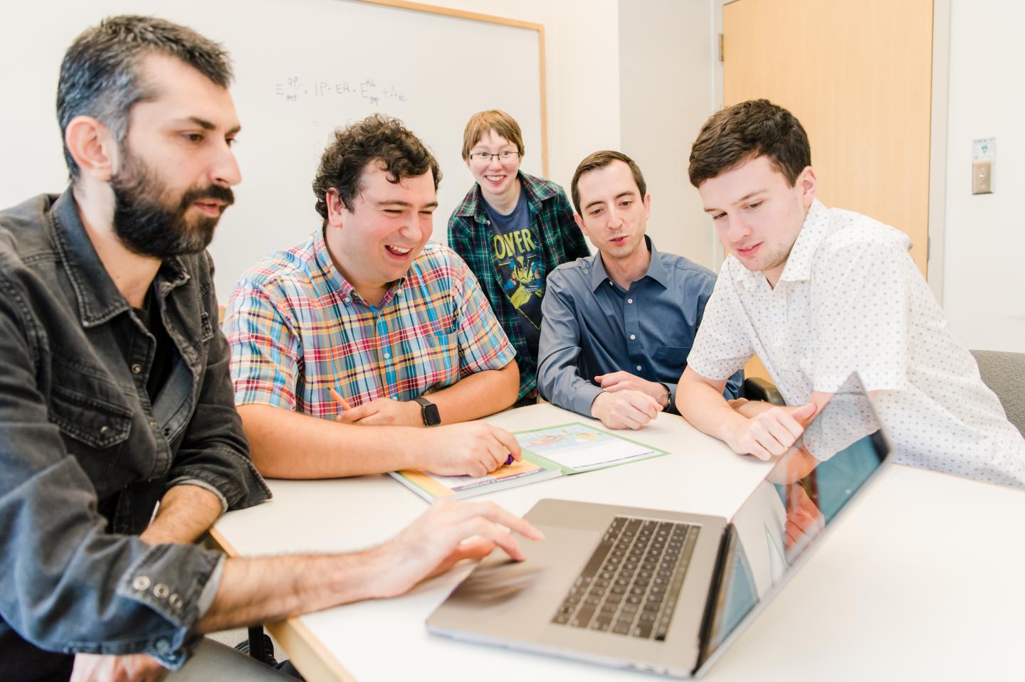
New research by Daniel Wines, Ph.D. candidate in physics, and Ataca gives those scientists the information they need to pursue high-impact research in this field. Their theoretical work provides reliable information about which new materials might have desirable properties for a range of applications and could exist in a stable form in nature. In a recent paper published in ACS Applied Materials and Interfaces, they used cutting-edge computer modeling techniques to predict the properties of 2D materials that haven’t yet been made in real life.
“We usually are trying to stay five or so years ahead of experimentalists,” says Wines. That way, they can avoid going down expensive dead ends. “That’s time, effort, and money that they can focus on other things.”
The perfect mix
The new paper focuses on the stability and properties of 2D materials called group III nitrides. These are mixtures of nitrogen and an element from group III on the periodic table, which includes aluminum, gallium, indium, and boron.
Scientists have already made some of these 2D materials in small quantities. Instead of looking at mixtures of one of the group III elements with nitrogen, however, Wines and Ataca modeled alloys–mixtures including nitrogen and two different group III elements. For example, they predicted the properties of materials made of mostly aluminum, but with some gallium added, or mostly gallium, but with some indium added.
These “in-between” materials might have intermediate properties that could be useful in certain applications. “By doing this alloying, we can say, I have orange light, but I have materials that can absorb red light and yellow light,” Ataca says. “So how can I mix that so that it can absorb the orange light?” Tuning the light absorption capabilities of these materials could improve the efficiency of solar energy systems, for example.
Alloys of the future
Ataca and Wines also looked at the electric and thermoelectric properties of materials. A material has thermoelectric capability if it can generate electricity when one side is cold and the other is hot. The basic group III nitrides have thermoelectric properties, “but at certain concentrations, the thermoelectric properties of alloys are better than the basic group III nitrides,” Ataca says.
Wines adds, “That’s the main motivation of doing the alloying–the tunability of the properties.”
They also showed that not all of the alloys would be stable in real life. For example, mixtures of aluminum and boron at any concentrations were not stable. However, five different ratios of gallium-aluminum mixtures were stable.
Once production of the basic group III nitrides becomes more reliable and is scaled up, Wines and Ataca expect scientists to work on engineering the materials for specific applications using their results as a guide.
Back to basics…with supercomputers
Wines and Ataca modeled the materials’ properties using supercomputers. Rather than using experimental data as input for their models, “We are using the basics of quantum mechanics to create these properties. So the good part is we don’t have any experimental biases,” Ataca says. “We’re working on stuff that doesn’t have any experimental evidence before. So this is a trustable approach.”
To get the most accurate results requires huge amounts of computing power and takes a long time. Running their models at the highest accuracy level can take several days.
“It’s kind of like telling a story,” Wines says. “We go through the most basic level to screen the materials,” which only takes about an hour. “And then we go to the highest levels of accuracy, using the most powerful computers, to find the most accurate parameters possible.”
“I think the beautiful part of these studies is that we started at the basics and we literally went up to the most accurate level in our field,” Ataca adds. “But we can always ask for more.”
A new frontier
They have continued to move forward into uncharted scientific territory. In a different paper, published within a week of the first in ACS Applied Materials and Interfaces, Theodosia Gougousi, professor of physics; Jaron Kropp, Ph.D. ’20, physics; and Ataca demonstrated a way to integrate 2D materials into real devices.
2D materials often need to attach to an electronic circuit within a device. An in-between layer is required to make that connection–and the team found one that works. “We have a molecule that can do this, that can make a connection to the material, in order to use it for external circuit applications,” Ataca says.
This result is a big deal for the implementation of 2D materials. “This work combines fundamental experimental research on the processes that occur on the surface of 2D atomic crystals with detailed computational evaluation of the system,” Gougousi says. “It provides guidance to the device community so they can successfully integrate novel materials into traditional device architectures.”
Collaboration across disciplines
The theoretical analyses for this work happened in Ataca’s lab, and the experiments happened in Gougousi’s lab. Kropp worked in both groups.
“The project exemplifies the synergy that is required for science and technology development and advancement,” Gougousi says. “It is also a great example of the opportunities that our graduate students have to work on problems of great technological interest, and to develop a broad knowledge basis and a unique set of technical skills.”
Kropp, who is first author on the second paper, is thrilled to have had this research experience.
“2D semiconductors are exciting because they have the potential for applications in non-traditional electronic devices, like wearable or flexible electronics, since they are so thin,” he says. “I was fortunate to have two excellent advisors, because this allowed me to combine the experimental and theoretical work seamlessly. I hope that the results of this work can help other researchers to develop new devices based on 2D materials.”
###
Media Contact
Sarah Hansen
[email protected]
Original Source
https:/
Related Journal Article
http://dx.


