Credit: Chalmers University of Technology/Daniel Andren
In the future, camera lenses could be thousands of times thinner and significantly less resource-intensive to manufacture. Researchers from Chalmers University of Technology, Sweden, now present a new technology for making the artificial materials known as ‘metasurfaces’, which consist of a multitude of interacting nanoparticles that together can control light. They could have great use in the optical technology of tomorrow.
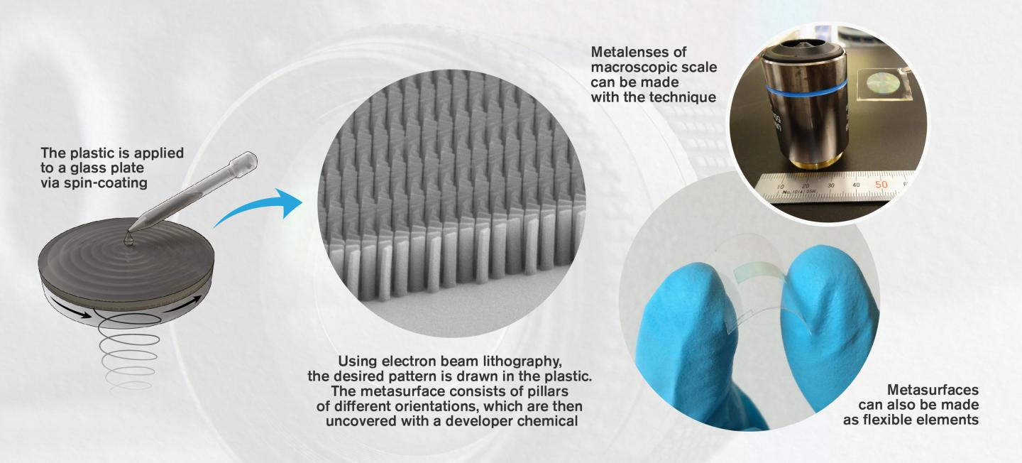
Metasurfaces can be used for optical components in portable electronics, sensors, cameras or space satellites. The Chalmers researchers’ new technology for making such planar surfaces is based on a plastic that is already used today to create other microstructures.
“We put a thin layer of this plastic on a glass plate and, using a well-established technique called electron-beam lithography, we can draw detailed patterns in the plastic film, which after development will form the metasurface. The resulting device can focus light just like a normal camera lens, but it is thousands of times thinner – and can be flexible too,” says Daniel Andrén, a PhD student at the Department of Physics at Chalmers and first author of the scientific article recently published in the journal ACS Photonics.
Over the past ten years, there has been a revolution in optics. The phones in our pockets have cameras comparable to a DSLR – technological masterpieces with millions of pixels of resolution. They process light with small advanced computer chips and software, and the image is recreated with the help of small coloured LEDs. These technologies have developed extremely rapidly in recent years, due mainly to smaller and more effective circuit components.
However, camera lenses themselves have not changed as much. The majority of today’s lenses are based on the same physical principles, and include the same basic limitations, as the first prototypes invented in the sixteenth century. In the past decade, however, researchers have begun to work with artificial materials – metasurfaces – that could replace today’s lenses.
Currently, certain issues stand in the way of large-scale manufacturing of metasurfaces. Advanced equipment is required to manufacture them, and the process is also very time-consuming. But using the Chalmers researchers’ new method, the production rate can be increased several times compared to current state-of-the-art techniques. The new technology uses harmless chemicals, as well as machines that are already common in nano-manufacturing laboratories today, meaning that more researchers could now begin to study metasurfaces.
“Our method could be a step towards large-scale production of metasurfaces. That is the goal we are already working towards today. Metasurfaces can help us create different effects and offer various technological possibilities. The best is yet to come,” says Ruggero Verre, a researcher at the Department of Physics at Chalmers and co-author of the scientific article.
###
Read the article Large-Scale Metasurfaces Made by an Exposed Resist, recently published in ACS Photonics, written by Daniel Andrén, Jade Martínez-Llinàs, Philippe Tassin, Mikael Käll and Ruggero Verre, who all work at the Department of Physics at Chalmers.
https:/
The research was funded by the Nano Excellence Initiative at Chalmers University of Technology, the Swedish Research Council and the Knut and Alice Wallenberg Foundation. The project utilised the nanofabrication and computation facilities at Myfab and SNIC.
For more information contact:
Daniel Andrén
PhD student, Department of Physics, Chalmers University of Technology, +46 31 772 45 40, [email protected]
Ruggero Verre
Researcher, Department of Physics, Chalmers University of Technology, +46 31 772 80 39, [email protected]
Media Contact
Joshua Worth
[email protected]
Related Journal Article
http://dx.


