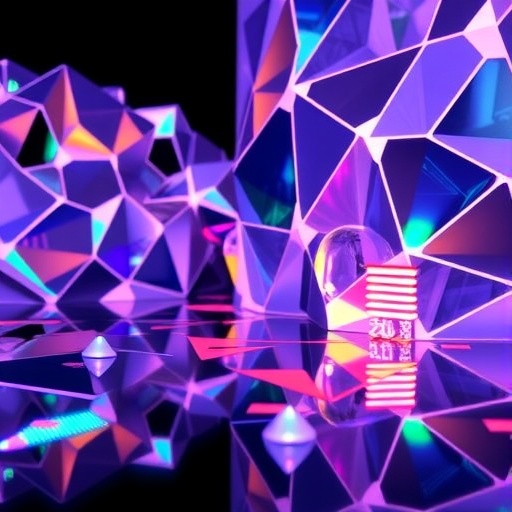
In the realm of nanophotonics, the precise manipulation of light at the nanoscale remains one of the most challenging yet promising frontiers. Optical Fourier surfaces, a class of intricately nanostructured gratings, have emerged as transformative elements capable of redistributing light across specific directions and wavelengths. These surfaces are poised to revolutionize compact spectrometers, augmented reality (AR) displays, and next-generation optical sensors due to their ability to engineer light-matter interactions with unprecedented spatial and angular specificity. However, the journey from design to real-world application has been hindered by the limitations intrinsic to conventional simulation methodologies. Typically, these approaches assume idealized conditions such as unidirectional illumination and flawless fabrication, which starkly contrast with practical, experimentally fabricated devices. This disconnect has long impeded the translation of theoretical designs into functional optical components with predictable performance.
Conventional nanophotonic design relies heavily on computational models like finite-difference time-domain (FDTD) simulations, which, despite their sophistication, are computationally intensive and often unstable when navigating the complex parameter spaces introduced by oblique and azimuthal illumination angles. The intrinsic assumptions of perfect geometry and single-angle incidence further undermine their accuracy; real-world devices invariably exhibit surface roughness, asymmetries, fabrication-induced imperfections, and ambient noise effects. Such discrepancies are particularly pronounced when design strategies exploit the angular degree of freedom—a powerful but underutilized parameter. By varying the incidence angle of incoming light, it is possible to selectively activate or suppress specific optical modes without any change to the physical structure, enabling multifunctional operation on a single device platform. This angular tuning expands the design landscape but simultaneously exacerbates the computational burden, rendering traditional simulation approaches increasingly impractical for iterative design and rapid prototyping.
Addressing this critical bottleneck, researchers at the Singapore University of Technology and Design (SUTD), in collaboration with colleagues from Xiamen University and Hefei University of Technology, have pioneered a reality-infused deep learning framework that fundamentally reimagines the design process for optical Fourier surfaces. Their approach circumvents the traditional reliance on physics-based simulations by leveraging extensive experimental datasets to train an advanced transformer-based neural network model dubbed ExpForm. This AI-driven methodology is grounded directly in empirical measurements rather than idealized theoretical constructs, enabling it to encapsulate the nuanced behavior of fabricated nanostructures under diverse angular conditions. This paradigm shift towards experiment-informed AI modeling signifies a major leap forward, offering both enhanced fidelity and computational efficiency.
The core data underpinning this breakthrough was amassed via a sophisticated high-throughput, angle-resolved spectroscopy system. This apparatus captures broadband reflectance spectra over a comprehensive matrix of incident angles—incorporating both polar and azimuthal variations—thereby mapping the full angular spectral response of the samples. Over 25,000 spectral instances were collected from four distinct quasi-optical Fourier surface samples fabricated through nanoimprint lithography, a technique that inherently introduces realistic fabrication features such as nanoscale roughness and structural asymmetries. By embedding the real-world imperfections and measurement noise into the training set, the model inherently accounts for complexities that elude conventional computational simulation, substantially enhancing predictive reliability.
The ExpForm framework operates through a dual-network design paradigm. The forward network ingests structural parameters and illumination angle data to predict reflectance spectra in real-time, achieving an unprecedented 99.79% consistency with experimental measurements. Conversely, the inverse network functions to unravel the design conundrum in reverse: given a target spectral response, it deduces the requisite nanostructure geometry and illumination conditions necessary to realize that response. The synergy of these dual capabilities forms an end-to-end design engine that obviates the traditional, labor-intensive iterative cycle of simulate-fabricate-measure-repeat. This not only accelerates the design timeline dramatically—demonstrating a roughly 900-fold speedup compared to conventional FDTD simulations—but also alleviates the dependency on costly fabrication processes.
This technology’s impact extends beyond computational expediency. The inverse design protocol empowers engineers to tailor nuanced optical phenomena on demand, including the generation of narrowband resonances at targeted wavelengths, custom high-reflectance profiles, and dual-band resonance functionalities. Remarkably, many of these sophisticated spectral manipulations are realized solely through angular tuning of the incident light, circumventing the need to fabricate multiple, structurally variant samples. This angle-driven programmable functionality heralds the advent of versatile nanophotonic devices capable of multifaceted operation within a single, static physical structure, radically enhancing device adaptability and applicability.
Dr. Dong Zhaogang, associate professor at SUTD and lead investigator of the study, emphasizes the conceptual importance of this advance. He notes that the approach transcends the traditional physics-first paradigm, embodying a data-informed, experimentally grounded design ethos wherein artificial intelligence acts as a co-designer rather than a passive computational tool. This shift opens new vistas not only in photonics but also across related disciplines such as materials science, quantum device engineering, and nanoelectronics, where complex, multi-parameter design landscapes similarly challenge existing methodologies.
Furthermore, the team’s commitment to open science is exemplified by their decision to release the complete experimental training dataset publicly. This unprecedented accessibility aims to democratize research in the nanophotonics community, fostering fair benchmarking and galvanizing innovation across various AI model architectures. Notably, while AI-driven experiment-based modeling has garnered success in microwave frequencies, this work pioneers its extension into the visible and near-infrared optical regimes, domains critical for consumer electronics, biomedical instrumentation, and communication technologies.
Looking ahead, the researchers envision broadening these methodologies to encompass high-quality-factor (high-Q) resonators, nonlinear photonic platforms, and three-dimensional metastructures exhibiting both in-plane and out-of-plane degrees of freedom. Early demonstrations have already validated the framework’s applicability to dielectric devices driven by bound states in the continuum, a class of resonances that promise ultra-high performance. Such expansions will further diversify the design landscape, enabling complex spectral and angular control strategies previously considered untenable due to computational or fabrication constraints.
Ultimately, this innovative synergy of experimental rigor, deep learning, and nanofabrication harbors transformative potential. It paves the way for agile, multifunctional optical devices capable of on-demand, angle-programmable operations, thereby catalyzing advances from fundamental science to cutting-edge technology deployment. As this reality-infused AI design paradigm matures, it will likely become a cornerstone of future photonic innovation and its allied fields.
Subject of Research: Optical Fourier surfaces and AI-driven design of nanophotonic devices
Article Title: Reality-infused deep learning for angle-resolved quasi-optical Fourier surfaces
Web References: https://doi.org/10.1186/s43074-026-00238-2
Image Credits: SUTD
Keywords
Photonics, Applied optics, Diffraction, Holography, Optical Fourier surfaces, Deep learning, Nanophotonics, Angle-resolved spectroscopy, AI inverse design, Transformer neural networks
Tags: AI in next-generation optical sensor developmentAI-driven design for augmented reality opticsAI-enhanced nanophotonics modelingcompact spectrometer optical surface optimizationhandling oblique illumination in nanophotonicslearning from real-world optical flawsnanophotonic optical Fourier surfacesnanostructured grating fabrication imperfectionsoptical surface roughness impact on performanceovercoming simulation limitations in nanophotonicsreal-world vs idealized optical simulationstraining AI for optical surface design


