• HOME
  • NEWS
  • EXPLORE
    • CAREER
      • Companies
      • Jobs
    • EVENTS
    • iGEM
      • News
      • Team
    • PHOTOS
    • VIDEO
    • WIKI
  • BLOG
  • COMMUNITY
    • FACEBOOK
    • INSTAGRAM
    • TWITTER
Saturday, February 7, 2026
BIOENGINEER.ORG
No Result
View All Result
  • Login
  • HOME
  • NEWS
  • EXPLORE
    • CAREER
      • Companies
      • Jobs
        • Lecturer
        • PhD Studentship
        • Postdoc
        • Research Assistant
    • EVENTS
    • iGEM
      • News
      • Team
    • PHOTOS
    • VIDEO
    • WIKI
  • BLOG
  • COMMUNITY
    • FACEBOOK
    • INSTAGRAM
    • TWITTER
No Result
View All Result
Bioengineer.org
No Result
View All Result
Home NEWS Science News Chemistry

Taking microelectronics to a new dimension

Bioengineer by Bioengineer
March 23, 2021
in Chemistry
Reading Time: 2 mins read
0
IMAGE
Share on FacebookShare on TwitterShare on LinkedinShare on RedditShare on Telegram

IMAGE

Credit: by Erik Hagen Waller, Julian Karst, and Georg von Freymann

Metallic microstructures are the key components in almost every current or emerging technology. For example, with the next wireless communication standard (6G) being established, the need for advanced components and especially antennas is unbroken. The drive to yet higher frequencies and deeper integration goes hand in hand with miniaturization and fabrication technologies with on-chip capability. Via direct laser writing – an additive manufacturing technology that offers sub-micron precision and feature sizes – highly sophisticated and integrated components come into reach. One big advantage of direct laser writing is that it is not limited to the fabrication of planar structures but enables almost arbitrary 3D microstructures. This dramatically increases the options available to component or device designers and offers vast potential for, e.g., antenna performance improvement: gain, efficiency and bandwidth are higher at lower feeding losses for 3D antennas compared to their planar counterparts. These advantages become even more pronounced the higher the frequency gets.

In a recent paper published in Light: Advanced Manufacturing, a team of scientists from the Fraunhofer ITWM, the Technische Universität Kaiserslautern and the Stuttgart University have developed a novel photosensitive material that enables direct fabrication of highly conductive microcomponents via direct laser writing.

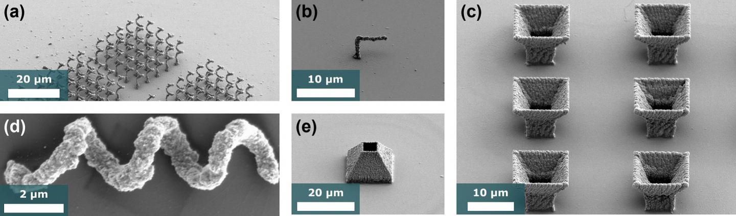
“Not only are the resulting structures made of almost 100 % silver, but they also have above 95% material density. Furthermore, almost arbitrary structure geometries are possible while onchip compatibility is maintained with this approach.”, says Erik Waller, the lead scientist of the project.

The feasibility and strength of the approach was demonstrated by the fabrication of a polarizer based on an array of helical antennas working in the infrared spectral region.

“This material and technology are well suited for the fabrication of conductive three dimensional micrometer-sized components. Next, we want to show the integration of thus fabricated components on conventionally fabricated chips. We then indeed take microelectronics to another dimension.”, says Georg von Freymann, head of department at the Fraunhofer ITWM and professor at the Technische Universität Kaiserslauten.

###

Media Contact
Erik Hagen Waller
[email protected]

Related Journal Article

http://dx.doi.org/10.37188/lam.2021.008

Tags: Chemistry/Physics/Materials SciencesOptics
Share12Tweet8Share2ShareShareShare2

Related Posts

blank

Breakthrough in Environmental Cleanup: Scientists Develop Solar-Activated Biochar for Faster Remediation

February 7, 2026
blank

Cutting Costs: Making Hydrogen Fuel Cells More Affordable

February 6, 2026

Scientists Develop Hand-Held “Levitating” Time Crystals

February 6, 2026

Observing a Key Green-Energy Catalyst Dissolve Atom by Atom

February 6, 2026
Please login to join discussion

POPULAR NEWS

  • Robotic Ureteral Reconstruction: A Novel Approach

    Robotic Ureteral Reconstruction: A Novel Approach

    82 shares
    Share 33 Tweet 21
  • Digital Privacy: Health Data Control in Incarceration

    63 shares
    Share 25 Tweet 16
  • Study Reveals Lipid Accumulation in ME/CFS Cells

    57 shares
    Share 23 Tweet 14
  • Breakthrough in RNA Research Accelerates Medical Innovations Timeline

    53 shares
    Share 21 Tweet 13

About

We bring you the latest biotechnology news from best research centers and universities around the world. Check our website.

Follow us

Recent News

Phage-Antibiotic Combo Beats Resistant Peritoneal Infection

Boosting Remote Healthcare: Stepped-Wedge Trial Insights

Barriers and Boosters of Seniors’ Physical Activity in Karachi

Subscribe to Blog via Email

Enter your email address to subscribe to this blog and receive notifications of new posts by email.

Join 73 other subscribers
  • Contact Us

Bioengineer.org © Copyright 2023 All Rights Reserved.

Welcome Back!

Login to your account below

Forgotten Password?

Retrieve your password

Please enter your username or email address to reset your password.

Log In
No Result
View All Result
  • Homepages
    • Home Page 1
    • Home Page 2
  • News
  • National
  • Business
  • Health
  • Lifestyle
  • Science

Bioengineer.org © Copyright 2023 All Rights Reserved.