Credit: Xiaotian Zhang/Penn State
Creating two-dimentional materials large enough to use in electronics is a challenge despite huge effort but now, Penn State researchers have discovered a method for improving the quality of one class of 2D materials, with potential to achieve wafer-scale growth in the future.
The field of 2D materials with unusual properties has exploded in the 15 years since Konstantin Novoselov and Andre Geim pulled a single atomic layer of carbon atoms off of bulk graphene using simple adhesive tape. Although a great amount of science has been conducted on these small fragments of graphene, industrial-sized layers are difficult to grow.
Of the materials envisioned for next-generation electronics, a group of semiconductors called transition metal dichalcogenides are at the forefront. TMDs are only a few atoms thick but are very efficient at emitting light, which makes them candidates for optoelectronics such as light-emitting diodes, photodetectors, or single-photon emitters.
“Our ultimate goal is to make monolayer films of tungsten diselenide or molybdenum disulfide sheets, and to deposit them using chemical vapor deposition in such a way that we get a perfect single crystal layer over an entire wafer,” said Joan Redwing, professor of materials science and electronics, and director of Penn State’s 2D Crystal Consortium, a National Science Foundation Materials Innovation Platform.
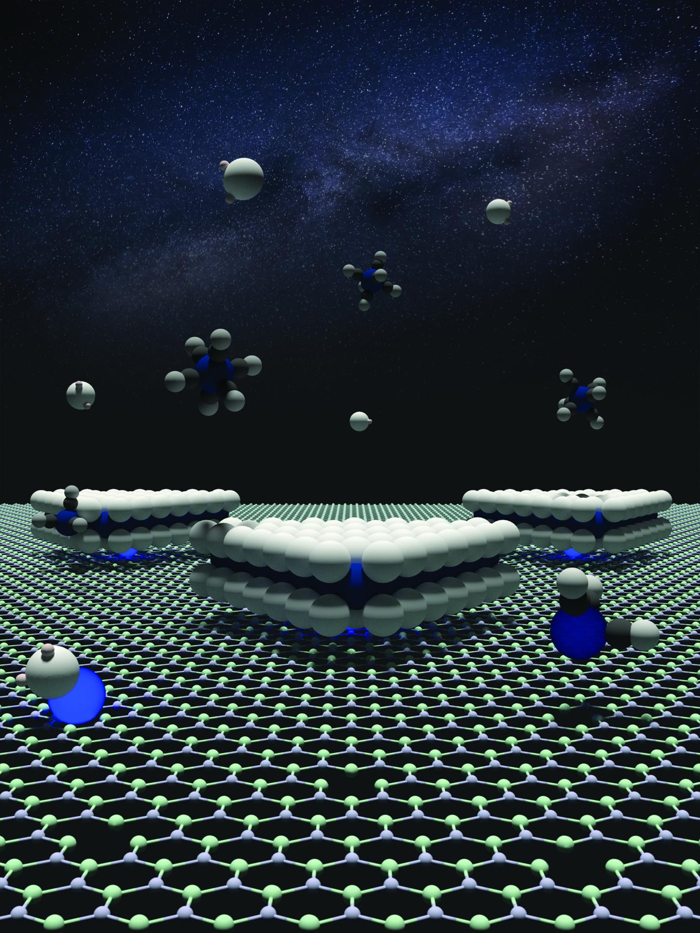
The problem comes from the way atoms organize themselves when they are deposited on a standard substrate, such as sapphire. Because of the crystal structure of TMDs, they form triangles as they begin to spread across the substrate. The triangles can be oriented in opposite directions, with equal probability. When they bump and merge into one another to form a continuous sheet, the boundary they form is like a large defect that drastically reduces the electronic and optical properties of the crystal.
“When the charge carriers, such as electrons or holes, encounter this defect, called an inversion domain boundary, they can scatter,” Redwing said. “This has been a classic problem with TMD growth.”
In recent publications in the journals ACS Nano and Physical Review B, researchers in Penn State’s Departments of Materials Science and Engineering, Physics, Chemistry, and Engineering Science and Mechanics show that if the TMDs are grown on a surface of hexagonal boron nitride, 85 percent or more will point in the same direction. Vin Crespi, distinguished professor of physics, materials science and engineering and Chemistry, and his group ran simulations to explain why this happened. They found that vacancies in the hexagonal boron nitride surface, where a boron or nitrogen atom was missing, could trap a metal atom – tungsten or molybdenum – and serve to orient the triangles in a preferred direction. The improved material showed increased photoluminescence emission and an order of magnitude higher electron mobility compared to 2D TMDs grown on sapphire.
“Our next step is to develop a process to grow hexagonal boron nitride across a wafer scale,” Redwing said. “That’s what we’re working on now. It’s difficult to control defects and to grow a single crystal layer across a large surface. Many groups are working on this.”
###
This work occurred in the facilities of the 2D Crystal Consortium Materials Innovation Platform, a National Science Foundation-supported national-user facility focused on advancing the synthesis of 2D materials. The user facility is open to all U.S. universities, government laboratories and industries.
Contributing authors on the ACS Nano paper, titled “Defect-controlled Nucleation and Orientation of WSe2 on hBN: A Route to Single-crystal Epitaxial Monolayers,” include Xiaotian Zhang and Fu Zhang, graduate students at the time the research was conducted; and professors Nasim Alem, Mauricio Terrones and Saptarshi Das, as well as Crespi and Redwing.
Contributing authors on the Physical Review B paper, titled “Full Orientation of Epitaxial MoS2 on hBN Assisted by Substrate Defects,” include lead authors Fu Zhang, research assistant professor, and recent doctoral graduate Yuanxi Wang.
Media Contact
A’ndrea Elyse Messer
[email protected]
Related Journal Article
http://dx.