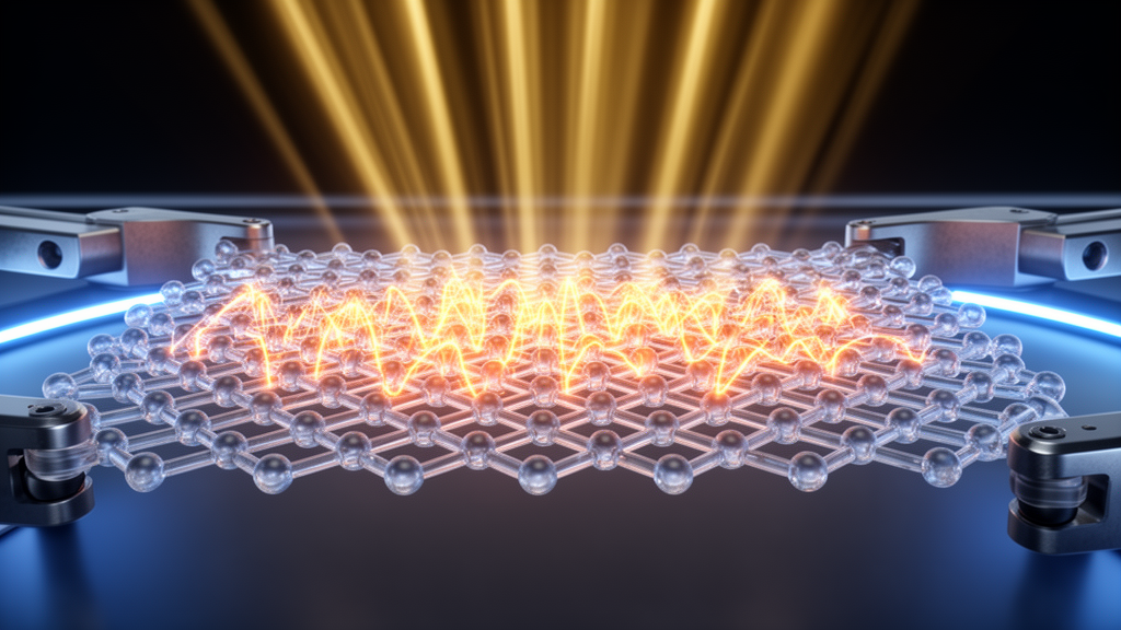
A single layer of atoms made from three of the lightest elements in the universe is emerging as one of the more intriguing candidates for the next generation of optoelectronic devices. In a study published in the Journal of Materials Science, Yuqing Dong and Huabing Shu of Jiangsu University of Science and Technology, together with Haiying Xu of the Nanjing Institute of Technology, report a comprehensive computational analysis of a new boron-carbon-nitride (BCN) monolayer. Using first-principles calculations that include many-body effects, the team found that the material is remarkably stable under a wide range of tensile strain and that stretching it can dramatically reshape its electronic and optical behavior. The findings suggest a route to devices whose light-absorbing properties could be dialed in simply by mechanical deformation, a concept known as strain engineering that has become one of the most active frontiers in two-dimensional materials research.
Two-dimensional materials have captivated physicists and engineers ever since graphene was first isolated, but the field has long faced a fundamental dilemma. Graphene itself is a superb conductor, yet it lacks a bandgap, the energy barrier that separates occupied from unoccupied electronic states and makes a material useful as a semiconductor. Hexagonal boron nitride, at the other extreme, is a wide-gap insulator. Sandwiching carbon between boron and nitrogen in a single atomic plane offers a tantalizing middle ground: a lattice built entirely from light elements that could, in principle, combine the robustness of boron nitride with semiconducting behavior suitable for transistors, photodetectors, and solar cells. The new study adds a fresh entry to this growing family of borocarbonitride compounds and subjects it to one of the most demanding tests a two-dimensional material can face: sustained mechanical stretching.
The researchers began by evaluating whether the proposed BCN lattice could exist at all. Stability is the perennial Achilles heel of hypothetical two-dimensional crystals, many of which look beautiful on paper but fall apart the moment their atomic vibrations are examined. To probe this, the team performed phonon analysis, a technique that calculates the full spectrum of vibrational modes in the crystal. If any of these modes have imaginary frequencies, the lattice is dynamically unstable and will spontaneously distort or disintegrate. The BCN monolayer passed this test convincingly, remaining dynamically stable not only in its pristine form but across a wide range of applied biaxial tensile strain. That resilience matters enormously for practical applications, because any real device built on a flexible substrate will subject its active layer to mechanical stress, and a material that cannot survive deformation is of little use in flexible electronics.
In its unstrained state, the pristine BCN monolayer exhibits a direct bandgap of approximately two electronvolts. A direct bandgap means that an electron dropping from the conduction band to the valence band can emit a photon without needing a change in momentum, which is precisely the property that makes materials like gallium arsenide valuable for LEDs and lasers. A gap of roughly two electronvolts places the material in the visible-light range, meaning it can absorb and potentially emit photons in the portion of the spectrum most relevant to human vision and to solar energy conversion. This combination of a direct gap and an all-light-element composition is rare, and it immediately positions the monolayer as a candidate for ultrathin, lightweight optoelectronic components.
The most striking results, however, emerged when the researchers applied biaxial tensile strain, uniformly stretching the lattice in both in-plane directions. The bandgap proved highly sensitive to this deformation, decreasing substantially as the strain increased. This behavior follows a well-established principle in semiconductor physics: stretching a lattice weakens and lengthens the bonds between atoms, which alters the overlap of their electronic orbitals and shifts the energies of the band edges. In many two-dimensional semiconductors, including the widely studied molybdenum disulfide, strain has been shown to modify the gap by hundreds of millielectronvolts. What makes the new BCN monolayer notable is the magnitude of the effect combined with the material’s demonstrated stability under the same conditions, meaning the tuning window can actually be exploited rather than merely observed before the crystal fails.
The optical consequences of this strain sensitivity are equally significant. The team calculated the material’s absorption spectrum and found it to be highly anisotropic, meaning it absorbs light differently depending on the polarization direction relative to the crystal axes. Anisotropic absorption is a valuable property for polarization-sensitive photodetectors, which can distinguish the orientation of incoming light and are used in imaging, sensing, and communications technologies. The prominent absorption peaks in the spectrum shifted to longer wavelengths, a redshift, as tensile strain increased, tracking the narrowing of the electronic bandgap. Because the gap defines the minimum photon energy the material can absorb, stretching the lattice effectively broadens the range of low-energy photons it can capture, pulling previously invisible parts of the spectrum into play.
Perhaps the most application-relevant finding concerns the near-infrared and visible regions of the spectrum. The calculations showed that light absorption in these bands, which are the workhorse ranges for photovoltaics, imaging, and telecommunications, can be effectively enhanced by applying tensile strain. In practical terms, a thin film of this material could be made a better solar absorber or a more sensitive infrared detector simply by stretching it, without any chemical doping or compositional change. Because strain can be applied dynamically, through flexible substrates, piezoelectric actuators, or patterned substrate topography, this opens the possibility of devices whose spectral response is actively adjustable in operation, a degree of freedom that conventional bulk semiconductors cannot offer.
The study also examined excitons, the bound pairs of photoexcited electrons and holes that form when light is absorbed in a semiconductor. In two-dimensional materials, reduced dielectric screening makes excitons exceptionally tightly bound, which is scientifically fascinating but technologically problematic: an exciton that will not separate cannot contribute its charges to a photocurrent. The researchers found that the exciton binding energy in the BCN monolayer is largely reduced as tensile strain increases. Weaker exciton binding facilitates the effective spatial separation of photoexcited electrons and holes, allowing the charge carriers to escape their mutual attraction and be collected as current. For photovoltaic and photodetector applications, this strain-induced reduction in binding energy could translate directly into improved conversion efficiency and faster response times.
Methodologically, the work stands out for its rigor. Rather than relying on standard density functional theory alone, which notoriously underestimates bandgaps and neglects excitonic effects, the team employed many-body perturbation theory in the GW and Bethe-Salpeter framework, the gold standard for predicting the excited-state properties of low-dimensional materials. They combined the QUANTUM ESPRESSO simulation suite with the Yambo code for excited-state calculations, using PBE exchange-correlation functionals and optimized norm-conserving pseudopotentials from the PseudoDojo database. This level of theoretical treatment is essential for obtaining trustworthy optical spectra and exciton energies, and it lends considerable weight to the quantitative predictions about strain tuning.
The broader significance of the study lies in its demonstration that light-element two-dimensional materials deserve the same strain-engineering attention that has been lavished on transition metal dichalcogenides. The authors frame their findings as both the discovery of a new member of the light-elemental two-dimensional family and an emphasis on its potential in strain-engineered optoelectronic devices. The work was supported by the National Natural Science Foundation of China and Jiangsu University of Science and Technology. As experimentalists continue to synthesize increasingly exotic borocarbonitride phases, from graphitic BCx compounds to hexagonal BC2N films grown by chemical vapor deposition, computational studies like this one serve as a map, pointing synthetic chemists toward the structures most likely to survive the journey from theory to working devices, and toward the mechanical tricks that could unlock their full optical potential.
Subject of Research: Strain-dependent stability and electro-optical properties of a two-dimensional boron-carbon-nitride monolayer
Article Title: Impact of biaxial tensile strain on stability and electro-optical properties of new B–C–N hybrid monolayer
Article References: Dong, Y., Shu, H., & Xu, H. (2026). Impact of biaxial tensile strain on stability and electro-optical properties of new B–C–N hybrid monolayer. Journal of Materials Science. https://doi.org/10.1007/s10853-026-13900-8
Image Credits: AI Generated
DOI: 10.1007/s10853-026-13900-8
Keywords: BCN monolayer, two-dimensional materials, biaxial tensile strain, bandgap engineering, first-principles calculations, many-body effects, exciton binding energy, optical absorption, strain engineering, optoelectronics, phonon stability, near-infrared
News Source: Denise Maddox. (October 8, 2026). Stretching a New Boron-Carbon-Nitride Monolayer Could Tune Its Light-Harvesting Power. Scienmag.