Credit: by Zhiwei Peng, Xiaolin Chen, Yulong Fan, David J. Srolovitz, Dangyuan Lei
Strain engineering usually refers to a kind of material processing technology, which aims to regulate the properties of materials or optimize related devices’ performance by inherent or external strain. In recent years, with the development of 2D materials, the research of strain engineering of 2D materials (transition metal dichalcogenides (TMDCs), graphene, etc.) has attracted significant attention. Compared with strain engineering of traditional bulk materials, the atomic thickness of 2D materials makes them more suitable to serve as the platform for strain-engineering research and builds a bridge between strain engineering and nanophotonics. Hence, they are worthy of attention in many points of view, from fundamental physics to practical applications.
In a new paper published in Light: Science & Applications, a team of scientists, led by Doctor Dangyuan Lei from Department of Materials Science and Engineering, City University of Hong Kong, China, and co-workers have written a review article to comprehensively summarized recent developments in this burgeoning field. In this review paper, the traditional macroscopic strain field theory is introduced firstly. Then, the band structure changes of strained 2D semiconductors (TMDCs) and strained graphene are discussed, while the optical responses observed under different kinds of strain fields are reviewed. Subsequently, this paper summarizes the strain engineering techniques that can apply different kinds of strains to specific 2D materials. At the end of this article, the diverse applications in optical devices, optoelectronics and other photonics applications are presented, and the existing problems in this field and their future development are prospected, respectively.
Traditional strain engineering mainly focuses on silicon, germanium and other 3D bulk materials, which usually lack high fracture strength due to their intrinsic 3D properties. Therefore, the rising 2D materials with atomic thickness (such as graphene, TMDCs) have entered the field of vision. Their strain engineering has been widely studied in both the scientific community and industrial society. Compared with the traditional 3D materials, the 2D characteristics of 2D materials endow them with some quite different and novel characteristics, making their strain engineering more attractive. These scientists summarize those unique properties of 2D materials:
“Based on the following three points, we think 2D materials as a perfect platform for strain engineering: (1) 2D materials have better mechanical properties (deformation capacity), which means they can sustain larger strain before fracture when compared to bulk materials; (2) 2D materials have better optical properties due to their strong exciton effects, which benefits their further applications in photonics devices; and (3) 2D materials have more variable deformation patterns. Their atomic thickness properties allow them to achieve out-of-plane strain, which is almost impossible in 3D bulk materials, allowing 2D materials to possess more deformation patterns, such as uniaxial and biaxial in-plane strain, wrinkle, fold, and localized non-uniform strain.”
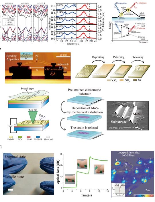
“Since the types of the applied strain are varied, the changes of electrical and optical properties are different. In general, we can observe the redshifted (blueshifted) PL spectra from the tensile (compressive) strained 2D TMDCs. Similarly, we can observe the shift and splitting of the Raman spectra from strained graphene. Besides, many novel optical responses, such as ‘funnel’ effect, single-photon emission and tunable second-harmonic generation, emerge under some special strain distribution.” they added.
“There are various technologies to apply strains to 2D materials. Based on the type of the induced strain, we usually classified them into three categories, namely, the uniaxial strain technologies, biaxial strain technologies and local strain technologies. We should pay more attention to local strain technologies. They actually give a new way to control photons in an ultrasmall area. In conclusion, the flexibility and optical properties of 2D materials (compared to their bulky counterparts) open the door for the development of potentially important new strain-engineered photonic applications.” the scientists forecast.
###
Media Contact
Dangyuan Lei
[email protected]
Related Journal Article
http://dx.


