Credit: by Xiaoxiao Sun, Ping Wang, Tao Wang, Ling Chen, Zhaoying Chen, Kang Gao, Tomoyuki Aoki, Li Mo, Jian Zhang, Tobias Schulz, Martin Albrecht, Weikun Ge, Yasuhiko Arakawa, Bo Shen, Mark…
Non-classical light sources such as single photon emitters are essential devices for the realization of future optical quantum technologies including optical quantum computing and quantum key distribution. To date several strategies, including single atoms, quantum dots (QDs), single molecules, and point defects, have been used to explore the development of single photon emitters. Although great strides have been made in the development of solid-state single photon emitters, including high purity and indistinguishability from QDs, and high emission rates from both defects and QDs, each technology has its own drawbacks. Therefore, basic research into the development of single photon emitters using new materials and techniques is crucial.
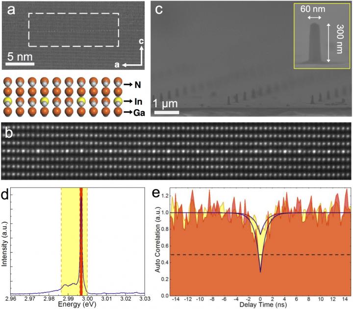
In a new paper published in Light Science & Applications, a team of scientists from State Key Laboratory for Mesoscopic Physics and Frontiers Science Center for Nano-optoelectronics, School of Physics, Peking University, China, and Institute of Industrial Science, The University of Tokyo, Japan have developed a novel type of quantum emitter formed from spatially separated monolayer islands of InGaN sandwiched in a GaN matrix. They first grew a planar structure of InGaN monolayer islands using molecular beam epitaxy, and then patterned the sample into pillars using nanoimprint lithography and inductively-coupled plasma reactive-ion etching. Detailed optical analysis of the emission properties of the isolated monolayer islands showed that the main emission line could be spectrally filtered to act as a bright, and fast single photon emitter at a wavelength of ~ 400 nm, with a high degree of photostability.
“III-nitride materials were chosen for this study because they are expected to offer several advantages for the development of future devices, including a wide tunability in emission wavelength, compatibility with silicon substrates for growth, and support from a worldwide industrial infrastructure for device fabrication due to their extended use in modern day optoelectronics and power device applications”, say the researchers.
The team also suggest that the next step in the research is to work towards higher emission purity, and that future developments (possibly using other materials) could lead to the realization of emitters operating at wavelengths compatible with conventional fiberoptic systems.
###
Media Contact
Xinqiang Wang
[email protected]
Related Journal Article
http://dx.


