Credit: by Urbonas, D., Mahrt, R.F. and Stöferle
For decades, the speed of our computers has been growing at a steady pace. The processor of the first IBM PC released 40 years ago, operated at a rate of roughly 5 million clock cycles per second (4.77 MHz). Today, the processors in our personal computers run around 1000 times faster.
However, with current technology, they’re not likely to get any faster than that.
For the last 15 years, the clock rate of single processor cores has stalled at a few Gigahertz (1 Gigahertz = 1 billion clock cycles per second). And the old and tested approach of cramming ever more transistors on a chip will no longer help in pushing that boundary. At least not without breaking the bank in terms of power consumption.
A way out of the stagnation could come in the form of optical circuits in which the information is encoded in light rather than electronics. In 2019, an IBM Research team together with partners from academia built the world’s first ultrafast all-optical transistor capable of operating at room temperature. The team now follows up with another piece of the puzzle, a silicon waveguide that links up such transistors, carrying light between them with minimal losses.
Wiring up the transistors of an optical circuit with silicon waveguides is an important requirement to make compact, highly integrated chips. That’s because it’s easier to place other needed components such as electrodes in its close vicinity if the waveguide is made of silicon. The techniques used for that purpose have been refined for decades in the semiconductor industry.
However, silicon being a notoriously strong absorber of visible light makes it great for capturing sunlight in a photovoltaics panels but a poor choice for a waveguide where light absorption means signal loss.
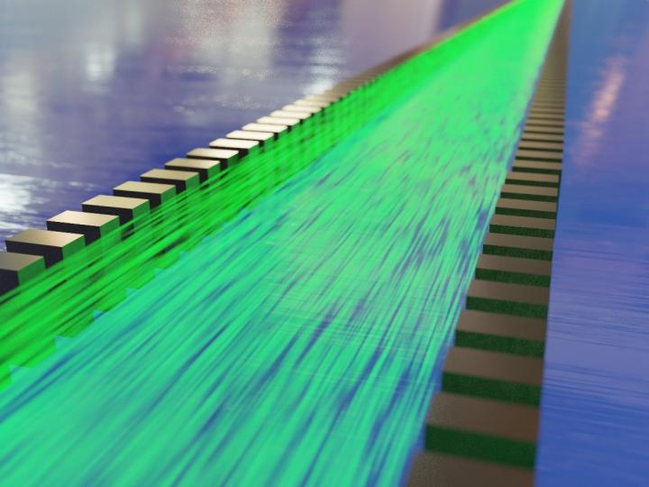
Making a fence to confine light
So, the IBM researchers thought of ways to use the mature silicon technology while circumventing the absorption issue. Their solution involves nanostructures called high contrast gratings with a striking behavior that some of the team members had already discovered over 10 years ago, albeit for another application.
A high contrast grating consists of nanometer sized “posts” lined up to form a sort of fence that prevents light from escaping. The posts are 150 nanometers in diameter and are spaced in such a way that light passing through the posts interferes destructively with light passing between posts. Destructive interference is a well-known phenomenon by which waves oscillating out of sync cancel each other out at a point in space. It affects light, which is an electromagnetic wave, just as it does sound and other types of wave. In this case, the destructive interference makes sure that no light can “leak” through the grating. Instead, most of the light gets reflected back inside the waveguide. The IBM researchers also showed that absorption of light inside the posts themselves is minimal. All this together translates in losses of only 13 percent along a light travel path of 1 millimeter inside the waveguide. For comparison: Along already only one hundredth of that distance (10 micrometers) in a pure silicon waveguide without the gratings, the losses would amount to 99.7 percent.
Simulations for precise grating design
On its face, the basic idea behind the high contrast gratings looks simple. However, it was indeed surprising when the researchers found out for the first time that they could keep light from being absorbed by a “dark” material like silicon.
Back in 2010, when they first observed the grating effect, it occurred in a laser microcavity which helped because the light amplification by the laser would compensate for the losses. Also, they had the light hitting the gratings at almost 90 degrees which is a sweet spot for the grating effect to kick in. But keeping the losses low in a waveguide without the benefit of the laser gain and at almost grazing light incidence was much more challenging.
To make sure their grating design would be up to the task, the team ran simulations showing how light propagation inside the waveguide would change with varying grating dimensions. They found out that the grating would provide efficient guiding of light over a broad band of wavelengths. All they needed to do was choose the right spacing between the grating posts and make the posts themselves to the right thickness within a precision margin of 15 nanometers. Using a standard silicon photonics fabrication process, those requirements proved manageable. In fact, the experiments confirmed what the simulations had predicted in terms of low loss for visible light in the range between 550 and 650 nanometers.
Potential benefits for optical circuits and beyond
The team found some evidence through simulations that this design can be used to make not only straight waveguides but also guide the light around corners. But they haven’t yet run the experiments to confirm this idea. Even if it proves feasible, some further optimization will be needed to keep the additional losses low in that case. Looking ahead, a next step will be to engineer the efficient coupling of the light out of the waveguides into other components. That will be a crucial step in the team’s multi-year exploratory research project with the goal of integrating the all-optical transistors they demonstrated in 2019 into integrated circuits capable of performing simple logic operations.
The team believes that their low-loss silicon waveguide could enable new photonic chip designs for use in biosensing and other applications that rely on visible light. It could also benefit the engineering of more efficient optical components such as lasers and modulators widely used in telecommunications.
###
Media Contact
Thilo Stöferle
[email protected]
Related Journal Article
http://dx.


