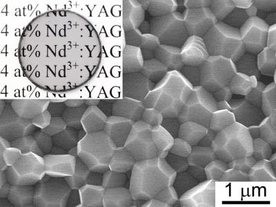
Credit: Denis Kosyanov, FEFU PI REC for Advanced Ceramic Materials Research
Scientists of Far Eastern Federal University (FEFU) have advanced the technology of high-speed sintering for optical ceramics (Nd3+:YAG), i.e. active elements generating laser emission in the near-infrared wavelength range (1.06 μm) for cutting the edge microelectronics and medicine. The researchers have managed to reduce significantly the initial nanopowders consolidation period (10 – 100 times) forming a nanostructure with ensured high optical transparency of the ceramic material. A related article appears in Optical Materials.
Diode-pumped microlasers based on Nd3+:YAG nanoceramics, due to their short lasing pulse duration, high peak power, and beam quality in combination with the elements’ small size, are relevant for the ranging, telecommunications, space technology, industry, and medicine.
Introduced a new approach to the technology of high-speed synthesis, young FEFU scientists achieved the optical quality of experimental ceramic materials at the level of world developments and commercial analogs. For that, they had combined the stages of the solid-state synthesis of the Nd3+:YAG structure from the initial Nd2O3, Y2O3, and Al2O3 oxide nanopowders, and its spark plasma sintering (SPS).
“The affectation of the SPS-technology is ceramics contaminates with carbon-containing impurities from the graphite parts of the set-up during sintering. For example, on carbides basis, new chemical compounds can form in the glassy and/or crystalline state, gas impurities, etc. Unwanted inclusions can dramatically reduce the transparency of optical materials and lead to the degradation of their mechanical characteristics. Our main task was to minimize or completely eliminate the formation of such impurities”, explains Anastasia Vornovskikh, junior researcher at the Advanced Ceramic Materials REC, Polytechnic Institute of Far Eastern Federal University.
Thanks to the SPS method, the total consolidation time for RE3+:YAG optical ceramics has been reduced by a factor of 10 – 100. Due to ultrafast sintering, the nanoscale of the grain structure of ceramics sustained provided their higher transparency in comparison with coarse-grained analogs. Their physical and mechanical properties as hardness, fracture toughness, plasticity, etc., significantly improved.
“In the context of the effect of carbon contamination, the team investigated all key sintering parameters such as heating rate, external pressure, temperature, and duration of sintering/post-annealing for transparency of Nd3+:YAG ceramics. We sew up a detailed sintering map to minimize the negative technological aspect. In general, in the case of suppressing carbon contaminations, the SPS technology acquires many advantages in comparison with conventional sintering technologies,” says Denis Kosyanov, FEFU research team lead, director of the FEFU PI REC for Advanced Ceramic Materials Research.
According to scientist, the most challenging thing turned out to be to determine the boundary parameters of the process where begins the chemical interaction of graphite impurities with the sintered material. Most of the analytical methods failed to apply due to the ultra-low content of these impurities. Only through a modern high-precision method of X-ray photoelectron spectroscopy, that is being jointly developed by the teams from FEFU, the Institute of Chemistry (FEB RAS), and the Institute for Single Crystals (NAS of Ukraine), it became possible for the first time to record the initial stage of carbonization during SPS of optical materials, describe its nature and mechanism.
As a result, an experimental high-doped 4 at% Nd3+:YAG transparent ceramics was synthesized. Its residual porosity is less than 0.02 vol%, in-line optical transmittance is about 87% of the theoretical value, microhardness of 13.2 GPa with average grain size is near 740 nm. The developers 3 times increased the level of doping of the garnet structure with neodymium ions in comparison with permissible values for the growth technologies of commercial Nd3+:YAG single crystals, preserving the nano grained structure and high mechanical characteristics of the material.
###
Scientists from FEFU, the Institute for Single Crystals (NAS Ukraine), the Institute of Chemistry and the Institute of Automation and Control Processes (FEB RAS), the Geophysical Survey of the RAS took part in the work.
Materials with controlled characteristics and providing new physical principles of operation of new generation microelectronics are one of the fastest-growing technological areas in the world and one of the priority areas in the development strategy of FEFU.
The study was supported by RFBR grant No. 18-29-11044 (scientific projects of interdisciplinary fundamental research “Ceramic materials for electronics and medicine”).
Media Contact
Alexander Zverev
[email protected]
Related Journal Article
http://dx.


