Scientists have developed a method for precise, fast and high-quality laser processing of halide perovskites, promising light-emitting materials for solar energy, optical electronics, and metamaterials
Credit: Small
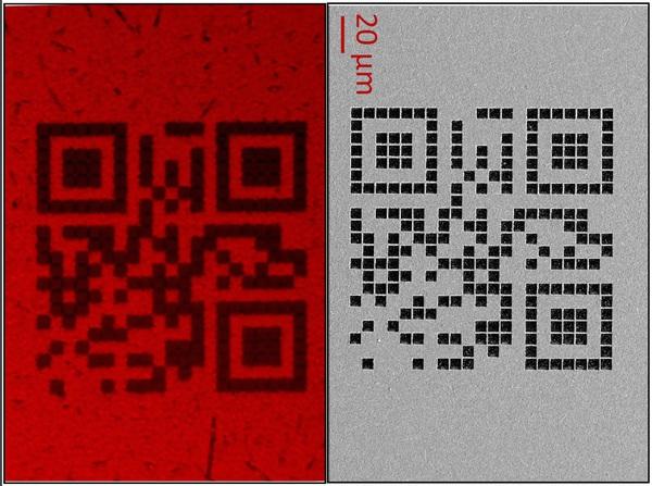
Scientists of Far Eastern Federal University (FEFU) in partnership with colleagues from ITMO University, and universities in Germany, Japan, and Australia, have developed a method for precise, fast and high-quality laser processing of halide perovskites (CH3NH3PbI3), promising light-emitting materials for solar energy, optical electronics, and metamaterials. Structured by very short laser pulses (femtosecond laser) perovskites turned out to be functional nanoelements marked by unprecedented quality. A related article is published in Small.
Perovskites were discovered in the first half of the 19th century in the Ural (Russia) in the form of a mineral consisting of calcium, titanium and oxygen atoms. Today, due to unique properties, perovskites are up-and-coming materials for solar energy and the development of light-emitting devices for photonics, i.e. LEDs and microlasers. They hit the top of the most scrutinizing materials that attract the interest of scientific groups from all around the world.
The major drawback is complicated processing. Perovskites easily degrade under the influence of an electron beam, liquids or temperature, losing the properties scientists are so interested in. This significantly complicates the manufacturing of functional perovskite nanostructures by means of common methods as electron beam lithography.
Scientists from FEFU (Vladivostok, Russia) and ITMO University (St. Petersburg, Russia) teamed up with foreign colleagues and solved this problem by proposing a unique technology for the processing of organo-inorganic perovskites using femtosecond laser pulses. The output was high-quality nanostructures with controlled characteristics.
“It is very difficult to nanostructurize conventional semiconductors, such as gallium arsenide, using a powerful pulsed laser,” says Sergey Makarov, a leading researcher at ITMO University’s Faculty of Physics and Engineering, “The heat is scattered in all directions and all the thin, sharp edges are simply distorted by this heat. It’s like if you try to make a miniature tattoo with fine details, but due to the paint spreading out under the skin, you will just get an ugly blue spot. Perovskite has poor thermal conductivity, so our patterns turned out very precise and very small.”
Laser scribing of perovskite films into individual blocks is an important technological step of the modern solar cell production chain. So far the process was not very accurate and being rather destructive for the perovskite material as its outermost sections lost functional properties due to temperature degradation. The new technology can help to solve this problem allowing fabrication of high-performing solar cells.
“Perovskite represents a complex material consisting of organic and inorganic parts. We used ultrashort laser pulses for fast heating and targeted evaporation of the organic part of perovskite that proceeds at rather low temperature of 160 C0. Laser intensity was adjusted in such a way to produce melting/evaporation of the organic part leaving inorganic one unaffected. Such nondestructive processing allowed us to achieve an unprecedented quality of produced perovskite functional structures”. Said one of the technology developers, Alexey Zhizhchenko, a researcher at the SEC “Nanotechnology” of FEFU School of Engineering.
Scientists of FEFU and ITMO University pointed to three areas where their development can give tangible results.
The first is the recording of information that the user can read under certain conditions only.
“We have demonstrated the relevance of our approach by producing diffraction gratings and microstrip lasers with the ultimately small width of only 400 nanometers. Such characteristic dimensions pave the way towards development of active elements of future optical communication chips and computers”. said Alexey Zhizhchenko.
Secondly, with the help of a laser, one can change the visible color of a perovskite fragment with no dye applied. Material may come like yellow, black, blue, red, depending on the needs.
“This may be utilized to perform solar panels of all colors of the rainbow. The modern architecture allows covering the entire surface of the building by solar panels, the point is not all customers want plain black panels”, Sergey Makarov said.
The third application is the manufacturing of nanolasers for optical sensors and optical chips which transmit information due to not the electrons flow but photons one.
Simple, fast and cost-effective production of such elements is to bring about a new era of computer technology working on the principles of controlled light. Processing of perovskites according to the proposed technology gives a chance to get thousands, even hundreds of thousands of nanolasers per minute. The introduction of the technology to the industry will draw the world closer to the development of optical computers.
“Another key feature of the proposed technology is that it allows layer-by-layer thinning of the perovskites. This opens the way to design and fabricate more complicated 3D microstructures from perovskite, for example, micro-scale vortex-emitting lasers, which are highly demanded for information multiplexing in next-generation optical communications. Importantly, such processing preserves and even improves the light-emitting properties of thinned layer passivated due to modification of chemical composition”, said team member Aleksandr Kuchmizhak, research fellow at the FEFU Center for Neurotechnology, VR and AR.
This study gathered specialists from FEFU, ITMO University, IAPC FEB RAS, Joint Institute for High Temperatures of the RAS, The Ruhr-University Bochum (Germany), Tokai University (Japan), and Swinburne University of Technology (Australia).
Previously, in the spring of 2019, a team of scientists from FEFU, ITMO University, The University of Texas at Dallas and The Australian National University developed an effective, fast and cheap way to fabricate perovskite microdisk lasers as promising sources of intense coherent light irradiation for optical microchips and optical computers of the new generation.
###
Media Contact
Alena Gupaisova
[email protected]
Related Journal Article
http://dx.


