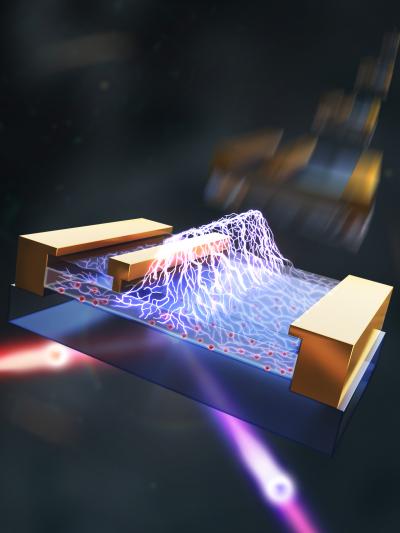
Researchers at the University of Bristol have discovered a method which will allow for faster communication systems and better energy saving electronics.
The breakthrough was made by establishing how to remotely measure the electric field inside a semiconductor device for the first time. A semiconductor is a material, such as Silicon, which can be used in electronic devices to control electric current.
Now, in this new study, published today in Nature Electronics, scientists outline how to precisely quantify this electric field, meaning next generation power and radio frequency electronic devices can be developed which have the potential to be faster, and more reliable, as well as more energy efficient.
Semiconductor device design can be trial and error, though more commonly it is based on a device simulation which then provides the basis for the manufacture of the semiconductor devices for real life applications. When these are new and emerging semiconductor materials, it has often been unknown how accurate and correct these simulations actually are.
Prof Martin Kuball of the University of Bristol’s School of Physics said: “Semiconductors can be made to conduct positive or negative charges and can therefore be designed to modulate and manipulate current. However, these semiconductor devices do not stop with Silicon, there are many others including Gallium Nitride (used in blue LEDs for example). These semiconductor devices, which for instance convert an AC current from a power line into a DC current, result in a loss of energy as waste heat – look at your laptop for example, the power brick is getting warm or even hot. If we could improve efficiency and reduce this waste heat, we will save energy.
“One applies a voltage to an electronic device, and as a result there is an output current used in the application. Inside this electronic device is an electric field which determines how this device works and how long it will be operational and how good its operation is. No one could actually measure this electric field, so fundamental to the device operation. One always relied on simulation which is hard to trust unless you can actually test its accuracy.”
To make good performance and long lasting electronic devices out of these new materials it is important that researchers find the optimal design, where electric fields do not exceed the critical value which would result in their degradation or failure. Experts plan to use newly emerging materials such as Gallium Nitride and Gallium Oxide rather than Silicon, allowing operation at higher frequency and at higher voltages, respectively, so that new circuits are possible which reduce energy loss. This work published by the University of Bristol group will provide an optical tool to enable the direct measurement of electric field within these new devices. This will underpin future efficient power electronics in applications such as solar or wind turbine stations feeding into the national grid, electric cars, trains and planes. Reduced energy loss means societies do not need to produce as much energy in the first place.
Prof Kuball said: “Considering that these devices are operated at higher voltages, this also means electric fields in the devices are higher and this in turn means they can fail easier. The new technique we have developed enables us to quantify electric fields within the devices, allowing accurate calibration of the device simulations that in turn design the electronic devices so the electric fields do not exceed critical limits and fail.”
Prof Kuball and his team plan to work with key industrial stake holders to apply the technique to advance their device technology. Within an academic context, they will engage with partners within the $12M US Department of Energy (DOE) ULTRA centre, they are partnered in, to use this technique to make ultra-wide bandgap device technology a reality, allowing energy savings in excess of 10% across the globe.
“This development helps the UK and the world to develop energy saving semiconductor devices, which is a step towards a carbon neutral society,” he added.
The technique was developed as part of an Engineering and Physical Sciences Research Council (EPSRC) project.
###
Paper
‘Electric field mapping of wide-bandgap semiconductor devices at a submicrometre resolution’ in Nature Electronics by Martin Kuball, Yuke Cao, James W Pomeroy, Michael J Uren and Feiyuan Yang
Media Contact
Laura Thomas
[email protected]