‘Suit of armour’ protects 2D materials for new-gen electronics
Credit: Phil Dooley ANU
An international team of scientists has invented the equivalent of body armour for extremely fragile quantum systems, which will make them robust enough to be used as the basis for a new generation of low-energy electronics.
The scientists applied the armour by gently squashing droplets of liquid metal gallium onto the materials, coating them with gallium oxide.
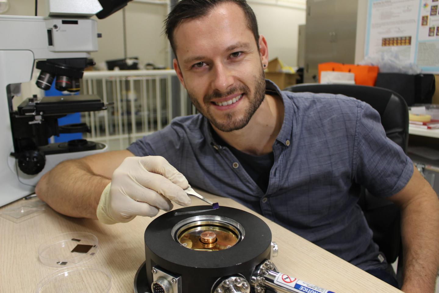
Protection is crucial for thin materials such as graphene, which are only a single atom thick – essentially two-dimensional (2D) – and so are easily damaged by conventional layering technology, said Matthias Wurdack, who is the lead author of the group’s publication in Advanced Materials.
“The protective coating basically works like a body armour for the atomically-thin material, it shields against high-energy particles, which would cause a large degree of harm to it, while fully maintaining its optoelectronic properties and its functionality,” said Mr Wurdack, a PhD student in the Nonlinear Physics Centre (NLPC) of the Research School of Physics, and the FLEET ARC Centre of Excellence.
The new technique opens the way for an industry based on ultra-thin electronics to expand, said leader of the research team, Professor Elena Ostrovskaya, also from NLPC and FLEET.
“Two-dimensional materials have extraordinary properties such as extremely low resistance or highly efficient interactions with light.”
“Because of these properties they could have big role in the fight against climate change.”
Eight percent of global electricity consumption in 2020, was due to information technologies, including computers, smartphones and large data centres of tech giants such as Google and Amazon. That figure is projected to double every decade as demand for AI services and smart devices skyrockets.
However, this work promises lower-energy alternatives for electronics and optoelectronics, by harnessing the superior performance of 2D semiconducting materials, such as tungsten disulphide, which was used in this study.
Using 2D materials to make more efficient devices will have advantages beyond reduced carbon emissions, says Mr Wurdack.
“2D technology could also enable super-efficient sensors on space craft, or processors in Internet of Things devices that are less limited by battery life.”
The team created their protective layer by exposing to air a droplet of liquid gallium, which immediately formed a perfectly even layer of gallium oxide on its surface a mere three nanometers thick.
By squashing the droplet on top of the 2D material with a glass slide, the gallium oxide layer can be transferred from the liquid gallium onto the material’s entire surface, up to centimetres in scale.
Because this ultrathin gallium oxide is an insulating amorphous glass, it conserves the optoelectronic properties of the underlying 2D semiconductor. The gallium oxide glass can also enhance these properties at cryogenic temperatures and protects well against other materials deposited on top. This allows the fabrication of sophisticated, layered nanoscale electronic and optical devices, such as light emitting diodes, lasers and transistors.
“We’ve generated a nice alternative to existing technology that can be scaled for industry applications,” Mr Wurdack said.
“We hope to find industry partners to work with us to develop a protective layer printer based on this technology, that can go into any lab, like a lithography machine.”
“It would be exciting to see fundamental research like this find its way into industry!”
###
THE STUDY
Ultrathin Ga2O3 Glass: A Large-Scale Passivation and Protection Material for Monolayer WS2 was published in Advanced Materials in December 2020. DOI 10.1002/adma.202005732
Media Contact
Errol Hunt
[email protected]
Related Journal Article
http://dx.


