Credit: Chao Xiang, UCSB
Optical frequency combs consist of light frequencies made of equidistant laser lines. They have already revolutionized the fields of frequency metrology, timing and spectroscopy. The discovery of ”soliton microcombs” by Professor Tobias Kippenberg’s lab at EPFL in the past decade has enabled frequency combs to be generated on chip. In this scheme, a single-frequency laser is converted into ultra-short pulses called dissipative Kerr solitons.
Soliton microcombs are chip-scale frequency combs that are compact, consume low power, and exhibit broad bandwidth. Combined with large spacing of comb “teeth”, microcombs are uniquely suited for a wide variety of applications, such as terabit-per-second coherent communication in data centers, astronomical spectrometer calibration for exoplanet searches and neuromorphic computing, optical atomic clocks, absolute frequency synthesis, and parallel coherent LiDAR.
Yet, one outstanding challenge is the integration of laser sources. While microcombs are generated on-chip via parametric frequency conversion (two photons of one frequency are annihilated, and a pair of two new photons are generated at a higher and lower frequency), the pump lasers are typically off-chip and bulky. Integrating microcombs and lasers on the same chip can enable high-volume production of soliton microcombs using well-established CMOS techniques developed for silicon photonics, however this has been an outstanding challenge for the past decade.
For the nonlinear optical microresonators, where soliton microcombs are formed, silicon nitride (Si3N4))has emerged as the leading platform due to its ultralow loss, wide transparency window from visible to mid-infrared, absence of two-photon absorption, and high power-handling capability. But achieving ultralow-loss Si3N4 microresonators is still insufficient for high-volume production of chip-scale soliton microcombs, as co-integration of chip-scale driving lasers are required.
Fifteen years ago, Professor John Bowers’s lab at UCSB pioneered a method for integrating semiconductor lasers onto a silicon wafer. Since silicon has an indirect bandgap and cannot emit light, scientists bond indium phosphide semiconductors on silicon wafers to form laser gain sections. This heterogeneous integration laser technology has now been widely deployed for optical interconnects to replace the copper-wire ones that linked servers at data centers. This transformative laser technology has been already commercialized, and Intel ships millions of transceiver products per year.
In an article published in Science, the two labs at EPFL and UCSB now demonstrate the first heterogenous integration of ultralow-loss Si3N4 photonic integrated circuits (fabricated at EPFL) and semiconductor lasers (fabricated at UCSB) through wafer-scale CMOS techniques.
The method is mainly based on multiple wafer bonding of silicon and indium phosphide onto the Si3N4 substrate. Distributed feedback (DFB) lasers are fabricated on the silicon and indium phosphide layers. The single-frequency output from one DFB laser is delivered to a Si3N4 microresonator underneath, where the DFB laser seeds soliton microcomb formation and creates tens of new frequency lines.
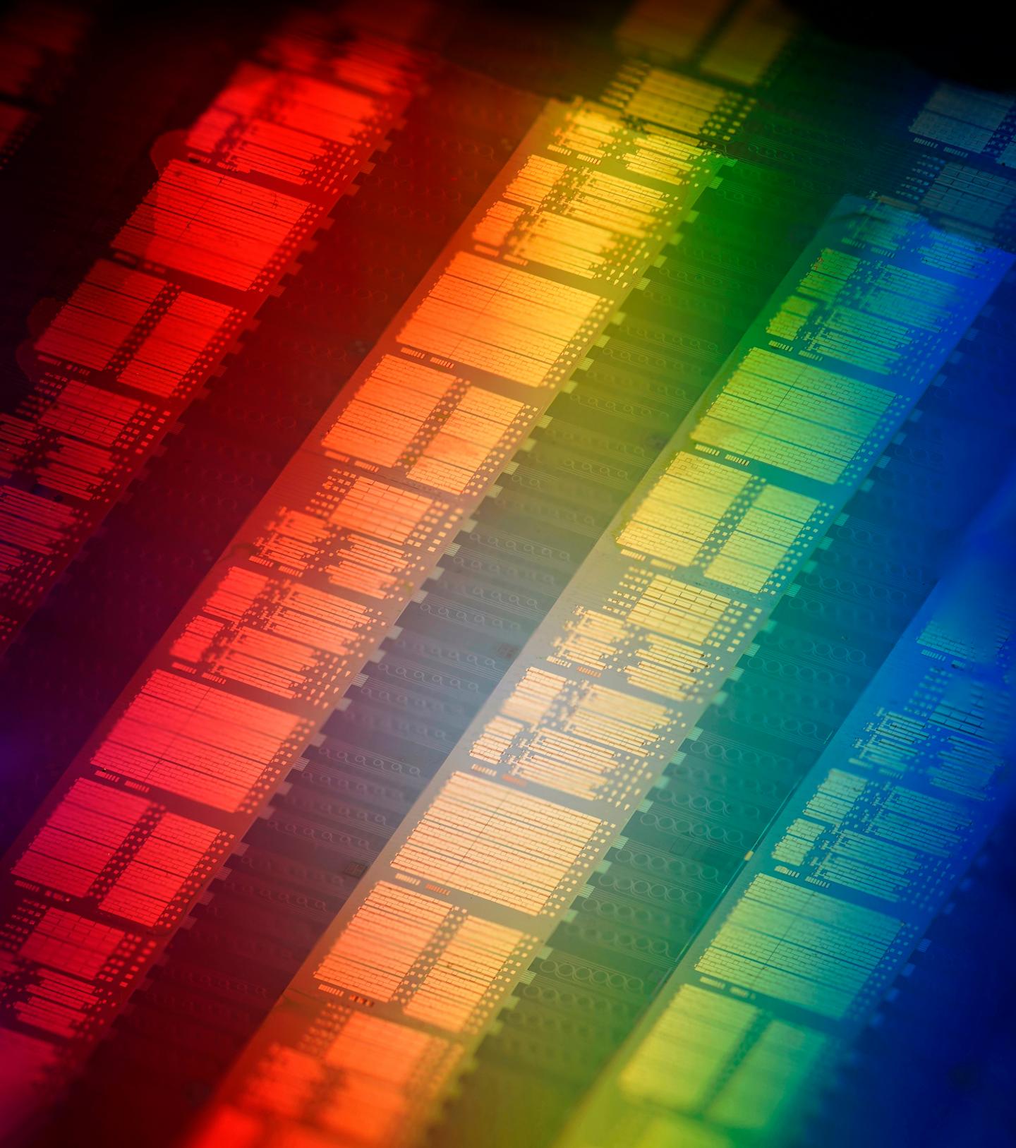
This wafer-scale heterogeneous process can produce more than a thousand chip-scale soliton microcomb devices from a single 100-mm-diameter wafer, lending itself to commercial-level manufacturing. Each device is entirely electrically controlled. Importantly, the production level can be further scaled up to the industry standard 200- or 300-mm-diameter substrates.
“Our heterogenous fabrication technology combines the three mainstream integrated photonics platforms, namely silicon, inidium phosphate and Si3N4, and can pave the way for large-volume, low-cost manufacturing of chip-based frequency combs for next-generation high-capacity transceivers, data centers, sensing and metrology,” says Dr Junqiu Liu who leads the Si3N4 fabrication at EPFL’s Center of MicroNanoTechnology (CMi).
###
Media Contact
Nik Papageorgiou
[email protected]


