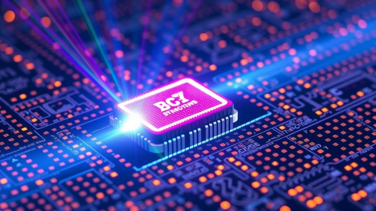
Researchers have unveiled a nanoscale optical memory that stores information permanently without any continuous power supply, using nothing more than light, silver, and a cleverly shaped cavity smaller than a bacterium. The design, reported in the journal Results in Optics by Melina Kehtarmanesh, Parviz Keshavarzi, and Mohammad Danaie, combines a metal-insulator-metal (MIM) plasmonic waveguide with the phase-change material Ge2Sb2Te5, better known as GST, the same alloy that has long been used in rewritable optical discs. The result is a single bit of non-volatile memory with an optical contrast of 95 percent, an extinction ratio of 25 decibels, and a footprint of just 0.095 square micrometers, corresponding to a storage density of 10.5 bits per square micrometer.
The motivation behind the work is the growing mismatch between the relentless growth of global data and the physical limits of electronic memory. Conventional silicon-based architectures, despite decades of refinement, are approaching hard boundaries in scalability, speed, and power density. All-optical memories, which encode, store, and retrieve information entirely within the optical domain, promise high transfer rates, low latency, and favorable energy efficiency. Yet each competing approach carries drawbacks: silicon-on-insulator platforms suffer from high losses, localized surface plasmon resonance structures are limited by ohmic losses and fabrication complexity, photonic crystals demand extreme fabrication precision, and Kerr nonlinear materials require high optical intensities and are sensitive to noise. Phase-change materials stand apart because they retain data even after the light source is removed, thanks to their non-volatile nature and high optical contrast between structural states.
The heart of the new device is a dumbbell-shaped resonator: a rectangular cavity flanked by two semi-disk resonators, coupled to MIM input and output waveguides carved in silver with air serving as the dielectric. Surface plasmon polaritons, hybrid waves of light and collective electron oscillations, are confined to the metal-dielectric interfaces and squeezed into regions far smaller than the wavelength of light. The team modeled the optical response of silver with the Drude formalism and validated the design using two-dimensional finite-difference time-domain (FDTD) simulations with a 3-nanometer mesh and perfectly matched layer boundaries. As a passive filter, the structure exhibits a Gaussian transmission peak at 1210 nanometers with a peak transmittance of 91 percent, a full width at half maximum of 56 nanometers, and a quality factor of about 21.
Geometry proved to be the decisive lever in tuning performance. Through systematic parametric sweep simulations, the researchers found that the radius of the semi-disk resonators dominates the resonance wavelength, shifting it by 2.22 nanometers for every nanometer of radius change, while the width of the rectangular cavity induces a blueshift at a sensitivity of minus 0.69 nanometers per nanometer, and the cavity length contributes a modest redshift of 0.3 nanometers per nanometer. The coupling gap between the waveguides and the resonator, varied from 0 to 18 nanometers, showed that transmission degrades progressively as the gap widens, because the evanescent field that transfers energy between the waveguide and the cavity decays exponentially with distance. Notably, the optimal configuration is a zero-gap, monolithic design, which sidesteps the notoriously difficult requirement of maintaining sub-10-nanometer alignment during fabrication.
Transforming this filter into memory required integrating a strip of GST, measuring 500 by 190 nanometers, into the central resonator and introducing a second optical pathway. A control signal, delivered from above the chip by a laser, programs the memory: a SET pulse of 50 milliwatts lasting 150 nanoseconds, roughly 7.5 nanojoules, gently heats the material above its crystallization temperature of about 450 kelvin, converting it from the amorphous to the crystalline state. A RESET pulse of 110 milliwatts for 20 nanoseconds, about 2.2 nanojoules, melts the material at roughly 880 kelvin before it rapidly quenches back into the amorphous phase. Crucially, this programming is spatially and functionally decoupled from the readout, which uses a low-power probe signal sent through the MIM waveguide, too weak to disturb the stored phase state.
The readout mechanism exploits the dramatic optical difference between the two phases of GST. In the amorphous state, the refractive index is 3.94 with low absorption, and the device transmits a resonance peak at 1912 nanometers with 95 percent transmittance, corresponding to logic state 1. In the crystalline state, both the real and imaginary refractive indices rise sharply to 6.11 plus 0.83i, absorption soars, and transmission drops to essentially zero, registering logic state 0. The contrast between the states reaches 95 percent, the extinction ratio reaches 25 decibels, and the insertion loss is a remarkably low 0.19 decibels in the amorphous state versus 25.2 decibels in the crystalline state. Because the phase persists without power, the bit is genuinely non-volatile, classifying the device within the PRAM and NVRAM families of memory.
The team went beyond static spectra and performed transient femtosecond-scale analysis using a square excitation pulse. In the amorphous state, the output rises to 95 percent of the input within about 200 femtoseconds after a 7-femtosecond propagation delay, with rise and fall times of 82 and 84 femtoseconds respectively, before ohmic losses drain the signal by roughly 1100 femtoseconds. In the crystalline state, the output settles at only about 4 percent, an OFF regime with minimal leakage. A reference simulation without the GST-loaded resonator confirmed that the MIM waveguides themselves preserve signal integrity with negligible distortion, meaning any temporal modification originates from the light-matter interaction inside the resonator. The researchers note that while these read dynamics reflect the electromagnetic impulse response rather than the slower phase-change kinetics, existing experimental literature supports GST switching frequencies between 1 and 10 megahertz with endurance up to one million cycles.
Perhaps the most forward-looking aspect of the design is its neuromorphic potential. The optical transmittance of the resonator is governed by the complex refractive index of the GST layer, and GST is well documented to undergo fractional crystallization, passing through intermediate states between fully amorphous and fully crystalline. Each intermediate state yields a distinct transmission level, which can be mapped onto an analog synaptic weight. The high-transmission amorphous state corresponds to a potentiated synapse, while the low-transmission crystalline state represents a depressed one. The authors frame the device as a scalable building block for all-optical neuromorphic synapses, potentially enabling spike-timing-dependent plasticity through tailored pulse-programming sequences in future circuits, thereby merging logic and memory on a single photonic platform in a departure from conventional von Neumann architectures.
Practical integration also received attention. The device is compatible with back-end-of-line CMOS processes, relying on standard techniques such as electron-beam evaporation, sputtering, electron-beam lithography, and reactive ion etching. The monolithic zero-gap resonant cavity can be patterned as a single continuous unit, eliminating fragile alignment steps, and sensitivity analysis confirms that performance peaks precisely at this configuration. Ultra-thin passivation layers of silicon dioxide or aluminum oxide can shield the silver from oxidation without compromising plasmonic confinement, while the high thermal conductivity of the silver substrate acts as a passive heat sink that, combined with nanosecond control pulses, suppresses thermal crosstalk. The authors acknowledge that the design deliberately prioritizes high transmission over an ultra-high quality factor, because the active GST layer introduces losses during switching and a strong baseline signal is essential for reliably distinguishing the two logic states. Compared against a broad field of plasmonic and photonic-crystal memories built on GST and Kerr materials, the proposed cell posts the highest transmission contrast in its class while remaining among the most compact, suggesting that light-written, power-free memory at the nanoscale may be moving from concept toward chip-ready reality.
Subject of Research: A non-volatile plasmonic memory based on an MIM waveguide and GST phase-change material for binary logic and neuromorphic computing
Article Title: Design of a non-volatile Plasmonic Memory Based on MIM waveguide and phase-change Materia for binary logic and neuromorphic integration
Article References: Kehtarmanesh, M., Keshavarzi, P., & Danaie, M. (2026). Design of a non-volatile Plasmonic Memory Based on MIM waveguide and phase-change Materia for binary logic and neuromorphic integration. Results in Optics, 25, Article 101141. https://doi.org/10.1016/j.rio.2026.101141
Image Credits: AI Generated
DOI: 10.1016/j.rio.2026.101141
Keywords: plasmonics, phase-change material, GST, non-volatile memory, MIM waveguide, optical memory, neuromorphic computing, photonic integrated circuits, FDTD simulation, optical contrast, synaptic weight, CMOS compatibility
Cite Scienmag News
APA MLA Chicago
Denise Maddox. (September 22, 2026). Plasmonic Memory Chip Uses Light and Phase-Change Material to Store Data Without Power. Scienmag. https://scienmag.com/plasmonic-memory-chip-uses-light-and-phase-change-material-to-store-data-without-power/
Denise Maddox. “Plasmonic Memory Chip Uses Light and Phase-Change Material to Store Data Without Power.” Scienmag, 22 September 2026, https://scienmag.com/plasmonic-memory-chip-uses-light-and-phase-change-material-to-store-data-without-power/. Accessed 22 September 2026.
Denise Maddox. “Plasmonic Memory Chip Uses Light and Phase-Change Material to Store Data Without Power.” Scienmag. September 22, 2026. https://scienmag.com/plasmonic-memory-chip-uses-light-and-phase-change-material-to-store-data-without-power/
Copy citation Download RIS
Tags: all-optical data storage technologyCMOS compatibilityFDTD simulationGSTGST phase-change alloyhigh-density optical memorylight-based data storagelight-driven memory devicesmetal-insulator-metal plasmonic waveguideMIM waveguidenanoscale optical data storageneuromorphic computingnon-volatile memorynon-volatile optical memoryoptical contrastoptical memoryovercoming electronic memory limitationsphase-change materialphase-change material data storagephotonic integrated circuitsplasmonic memory chipplasmonic nanostructures for memoryplasmonicssynaptic weight