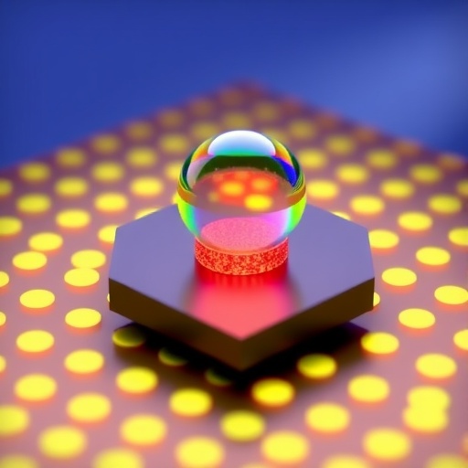
In a groundbreaking advancement in photonics, researchers from Wuhan University and Tsinghua University have pioneered a revolutionary platform that integrates topological exceptional points (EPs) within an all-dielectric, on-chip metasurface. This innovative strategy dispenses with traditional metallic components, thereby circumventing the notorious Ohmic losses associated with metal-based metasurfaces. By leveraging precise extraction methods for guided-wave optical fields, the study heralds a new era of compact, efficient, and highly integrable photonic devices, promising tremendous impacts on augmented reality (AR) visualization, optical information encoding, and next-generation optical display systems.
Metasurfaces, consisting of ultra-thin layers decorated with subwavelength meta-atoms, have long held promise for manipulating light at a fundamental level, enabling precise control over amplitude, phase, and polarization of optical waves. Their unique capacity to facilitate non-Hermitian physics, particularly the realization of topological EPs — points in parameter space where eigenvalues and eigenvectors coalesce — has been mostly demonstrated using metallic structures. However, metals inherently introduce undesirable energy dissipation via Ohmic losses, severely constraining device efficiency and hindering integration with purely dielectric photonic platforms.
Recognizing these constraints, the team spearheaded by Professor Zhongyang Li and Professor Qinghua Song has proposed and experimentally realized an all-dielectric on-chip metasurface capable of exciting topological EPs without resorting to metal components. Their approach ingeniously manipulates the geometry and spatial arrangement of dielectric meta-atoms atop dielectric waveguides to precisely extract and shape guided optical waves. This methodology not only eradicates absorption losses but also eliminates zero-order diffraction backgrounds, which often plague holographic projection systems and degrade image quality.
.adsslot_tIGZQyhV28{width:728px !important;height:90px !important;}
@media(max-width:1199px){ .adsslot_tIGZQyhV28{width:468px !important;height:60px !important;}
}
@media(max-width:767px){ .adsslot_tIGZQyhV28{width:320px !important;height:50px !important;}
}
ADVERTISEMENT
Central to their design is the selective generation and manipulation of left-handed circularly polarized (LCP) and right-handed circularly polarized (RCP) components. The research highlights an emergent topological singularity exclusively within the LCP channel, where amplitude and phase singularities coincide spatially, marking the presence of a topological exceptional point. Notably, such singular behavior is absent in the RCP component, a feature deftly exploited by the team to enable independent encoding and precise polarization decoupling through the synthesis of Pancharatnam-Berry phase modulation and topological phase accumulation around the EPs.
The practical realization of these principles culminated in a sophisticated on-chip meta-holography system that projects distinct holographic images—depicting a “Key” and a “Lock”—corresponding to LCP and RCP components, respectively. This dual-channel holographic encoding highlights the metasurface’s unparalleled capability for multiplexed optical information processing, a critical requirement for advanced photonic applications including data storage, secure communications, and dynamic displays.
Beyond mere demonstrations of optical manipulation, the platform’s robustness extends into augmented reality applications. Through an elaborate experimental configuration, AR images float vividly and distinctly above the real-world background without any parasitic visual artifacts. The suppression of undesired diffraction orders ensures unprecedented image clarity and fidelity, a key hurdle in translating holographic AR technology from laboratory concept to commercial wearable devices.
This research exemplifies the successful convergence of topological photonics with integrated on-chip dielectric platforms. It thereby expands the degrees of freedom available for optical system design, offering not only enhanced control over light-matter interaction but also compatibility with existing silicon photonics infrastructure. The all-dielectric configuration enables miniaturization and scalability, essential attributes for the commercialization of photonic chips in consumer electronics, optical computing, and quantum information processing.
Of particular note is the team’s ability to harness non-Hermiticity—an often challenging regime characterized by energy exchange with the environment—within a purely dielectric system. This contrasts sharply with prevailing approaches that rely on inherent losses from metallic elements. Their breakthrough paves the way for low-loss, tunable, and topologically robust photonic devices capable of sustaining exceptional point dynamics vital for sensing, lasing, and optical switching functionalities.
The metasurface’s waveguide integration marks a significant stride toward functional photonic circuits, as it allows seamless interplay between guided modes and free-space optical fields. By engineering the meta-atom shape and layout, the researchers achieve phase and amplitude control with extreme precision, leading to unparalleled manipulation of spatial and polarization degrees of freedom. Such versatility is indispensable for next-generation holographic displays, data multiplexing, and complex wavefront shaping.
Looking forward, the implications of this work are vast. The demonstrated all-dielectric topological metasurface could spearhead the development of compact, energy-efficient wearable AR devices offering superior image quality and interaction fidelity. Moreover, the platform’s ability to encode multiple optical channels independently holds promise for multiplexed information storage systems, setting new standards for data density and retrieval speed in photonic memory architectures.
In conclusion, this pioneering research melds the intricate physics of topological exceptional points with cutting-edge metasurface engineering to unlock new potentials in integrated photonics. By surmounting the loss-related limitations of metal-based systems through all-dielectric design, the team sets a formidable precedent for the creation of high-performance, scalable, and multifunctional optical devices that can redefine future technologies in AR, quantum photonics, and beyond.
Subject of Research: Topological exceptional points in all-dielectric on-chip metasurfaces and their applications in meta-holography and augmented reality.
Article Title: Creating topological exceptional point by on-chip all-dielectric metasurface
Web References:
10.1038/s41377-025-01955-2
Image Credits: Cheng Yi et al.
Keywords
Topological exceptional points, all-dielectric metasurface, on-chip photonics, non-Hermitian optics, guided-wave extraction, polarization decoupling, meta-holography, augmented reality, Pancharatnam-Berry phase, integrated photonic circuits, optical encoding, low-loss photonics
Tags: all-dielectric metasurfacesaugmented reality visualizationcompact photonic technologyefficient light manipulationenergy dissipation in photonicsguided-wave optical fieldsnext-generation optical displaysnon-Hermitian physicson-chip photonic devicesoptical information encodingsubwavelength meta-atomstopological exceptional points


