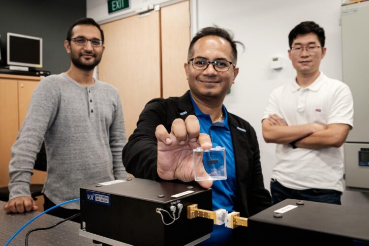
Credit: NTU Singapore
To enable data transmission speeds that surpass the 5th Generation (5G) standards for telecommunications, scientists from Nanyang Technological University, Singapore (NTU Singapore) and Osaka University in Japan have built a new chip using a concept called photonic topological insulators.
Published recently in Nature Photonics, the researchers showed that their chip can transmit terahertz (THz) waves resulting in a data rate of 11 Gigabits per second (Gbit/s), which is capable of supporting real-time streaming of 4K high-definition video, and exceeds the hitherto theoretical limit of 10 Gbit/s for 5G wireless communications.
THz waves are part of the electromagnetic spectrum, in between infrared light waves and microwaves, and have been touted as the next frontier of high-speed wireless communications.
However, fundamental challenges need to be tackled before THz waves could be used reliably in telecommunications. Two of the biggest issues are the material defects and transmission error rates found in conventional waveguides such as crystals or hollow cables.
These issues were overcome using Photonic Topological Insulators (PTI), which allows light waves to be conducted on the surface and edges of the insulators, akin to a train following railroads, rather than through the material.
When light travels along photonic topological insulators, it can be redirected around sharp corners and its flow will resist being disturbed by material imperfections.
By designing a small silicon chip with rows of triangular holes, with small triangles pointing in the opposite direction to larger triangles, light waves become “topologically protected”.
This all-silicon chip demonstrated it could transmit signals error-free while routing THz waves around 10 sharp corners at a rate of 11 gigabits per second, bypassing any material defects that may have been introduced in the silicon manufacturing process.
Leader of the project, NTU Assoc Prof Ranjan Singh, said this was the first time that PTIs have been realised in the terahertz spectral region, which proves the previously theoretical concept, feasible in real life.
Their discovery could pave the way for more PTI THz interconnects – structures that connect various components in a circuit – to be integrated into wireless communication devices, to give the next generation ‘6G’ communications an unprecedented terabytes-per-second speed (10 to 100 times faster than 5G) in future.
“With the 4th industrial revolution and the rapid adoption of Internet-of-Things (IoT) equipment, including smart devices, remote cameras and sensors, IoT equipment needs to handle high volumes of data wirelessly, and relies on communication networks to deliver ultra-high speeds and low latency,” explains Assoc Prof Singh.
“By employing THz technology, it can potentially boost intra-chip and inter-chip communication to support Artificial intelligence and cloud-based technologies, such as interconnected self-driving cars, which will need to transmit data quickly to other nearby cars and infrastructure to navigate better and also to avoid accidents.”
This project took the NTU team and their collaborators led by Professor Masayki Fujita at Osaka University two years of design, fabrication, and testing.
Prof Singh believes that by designing and producing a miniaturised platform using current silicon manufacturing processes, their new high-speed THz interconnect chip will be easily integrated into electronic and photonic circuit designs and will help the widespread adoption of THz in future.
Areas of potential application for THz interconnect technology will include data centres, IOT devices, massive multicore CPUs (computing chips) and long-range communications, including telecommunications and wireless communication such as Wi-Fi.
###
Note to Editor:
Paper titled “Terahertz topological photonics for on-chip communication”, published in Nature Photonics, 13 Apr 2020.
Media contact:
Lester Kok
Assistant Director
Corporate Communications Office
Nanyang Technological University
Email: [email protected]
About Nanyang Technological University, Singapore
A research-intensive public university, Nanyang Technological University, Singapore (NTU Singapore) has 33,000 undergraduate and postgraduate students in the Engineering, Business, Science, Humanities, Arts, & Social Sciences, and Graduate colleges. It also has a medical school, the Lee Kong Chian School of Medicine, established jointly with Imperial College London.
NTU is also home to world-renowned autonomous institutes – the National Institute of Education, S Rajaratnam School of International Studies, Earth Observatory of Singapore, and Singapore Centre for Environmental Life Sciences Engineering – and various leading research centres such as the Nanyang Environment & Water Research Institute (NEWRI) and Energy Research Institute @ NTU (ERI@N).
Ranked amongst the world’s top universities by QS, NTU has also been named the world’s top young university for the past seven years. The University’s main campus is frequently listed among the Top 15 most beautiful university campuses in the world and it has 57 Green Mark-certified (equivalent to LEED-certified) building projects, of which 95% are certified Green Mark Platinum. Apart from its main campus, NTU also has a campus in Singapore’s healthcare district.
Under the NTU Smart Campus vision, the University harnesses the power of digital technology and tech-enabled solutions to support better learning and living experiences, the discovery of new knowledge, and the sustainability of resources.
For more information, visit http://www.
Media Contact
Lester Kok
[email protected]
Original Source
https:/


