Transmorphic epitaxial growth of AlN nucleation layers on SiC substrates for high-breakdown thin GaN transistors
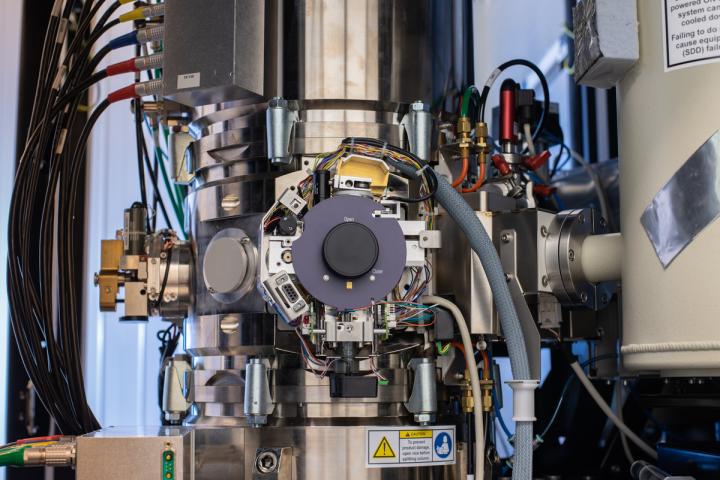
Credit: Magnus Johansson
A new method to fit together layers of semiconductors as thin as a few nanometres has resulted in not only a scientific discovery but also a new type of transistor for high-power electronic devices. The result, published in Applied Physics Letters, has aroused huge interest.
The achievement is the result of a close collaboration between scientists at Linköping University and SweGaN, a spin-off company from materials science research at LiU. The company manufactures tailored electronic components from gallium nitride.
Gallium nitride, GaN, is a semiconductor used for efficient light-emitting diodes. It may, however, also be useful in other applications, such as transistors, since it can withstand higher temperatures and current strengths than many other semiconductors. These are important properties for future electronic components, not least for those used in electric vehicles.
Gallium nitride vapour is allowed to condense onto a wafer of silicon carbide, forming a thin coating. The method in which one crystalline material is grown on a substrate of another is known as “epitaxy”. The method is often used in the semiconductor industry since it provides great freedom in determining both the crystal structure and the chemical composition of the nanometre film formed.
The combination of gallium nitride, GaN, and silicon carbide, SiC (both of which can withstand strong electric fields), ensures that the circuits are suitable for applications in which high powers are needed.
The fit at the surface between the two crystalline materials, gallium nitride and silicon carbide, is, however, poor. The atoms end up mismatched with each other, which leads to failure of the transistor. This has been addressed by research, which subsequently led to a commercial solution, in which an even thinner layer of aluminium nitride was placed between the two layers.
The engineers at SweGaN noticed by chance that their transistors could cope with significantly higher field strengths than they had expected, and they could not initially understand why. The answer can be found at the atomic level – in a couple of critical intermediate surfaces inside the components.
Researchers at LiU and SweGaN, led by LiU’s Lars Hultman and Jun Lu, present in Applied Physics Letters an explanation of the phenomenon, and describe a method to manufacture transistors with an even greater ability to withstand high voltages.
The scientists have discovered a previously unknown epitaxial growth mechanism that they have named “transmorphic epitaxial growth”. It causes the strain between the different layers to be gradually absorbed across a couple of layers of atoms. This means that they can grow the two layers, gallium nitride and aluminium nitride, on silicon carbide in manner so as to control at the atomic level how the layers are related to each other in the material. In the laboratory they have shown that the material withstands high voltages, up to 1800 V. If such a voltage were placed across a classic silicon-based component, sparks would start flying and the transistor would be destroyed.
“We congratulate SweGaN as they start to market the invention. It shows efficient collaboration and the utilisation of research results in society. Due to the close contact we have with our previous colleagues who are now working for the company, our research rapidly has an impact also outside of the academic world”, says Lars Hultman.
###
The research has been funded by research grants from the Knut and Alice Wallenberg Foundation and from the CoolHEMT programme, part of the EU Horizon 2020. The article, which is linked below, was specially selected by the editor of Applied Physics Letters, and is one of the journal’s most read articles, with nearly 1,000 downloads one week after publication on 25 November 2019. It is also featured on the journal´s cover.
Transmorphic Epitaxial Growth of AlN Nucleation Layers on SiC Substrates for High-Breakdown Thin GaN Transistors, Jun Lu, Jr-Tai Chen, Martin Dahlqvist, Riad Kabouche, Farid Medjdoub, Johanna Rosen, Olof Kordina, and Lars Hultman. Appl. Phys. Lett. 115, 221601 (2019). doi 10.1063/1.5123374
https:/
https:/
Media Contact
Professor Lars Hultman
[email protected]
Original Source
https:/
Related Journal Article
http://dx.


