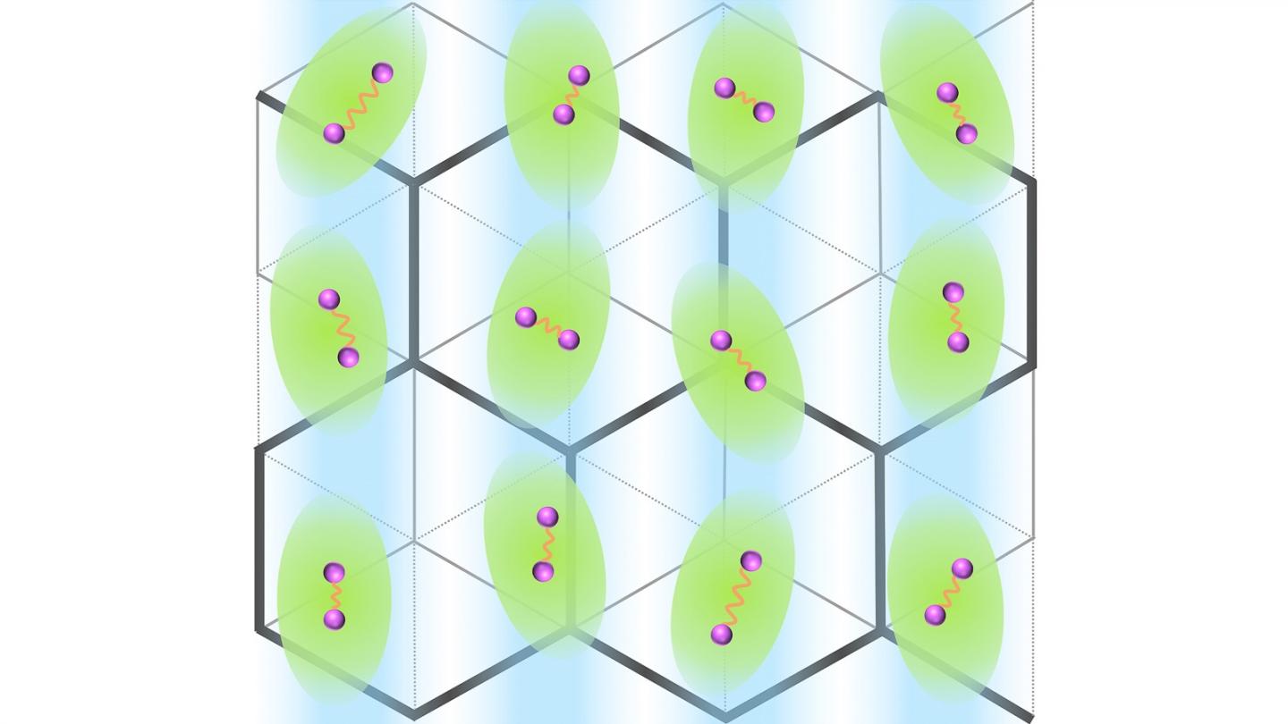
Credit: (Image by Anand Bhattacharya/Argonne National Laboratory.)
New interfacial superconductor has novel properties that raise new fundamental questions and might be useful for quantum information processing or quantum sensing.
Interfaces in solids form the basis for much of modern technology. For example, transistors found in all our electronic devices work by controlling the electrons at interfaces of semiconductors. More broadly, the interface between any two materials can have unique properties that are dramatically different from those found within either material separately, setting the stage for new discoveries.
Like semiconductors, superconducting materials have many important implications for technology, from magnets for MRIs to speeding up electrical connections or perhaps making possible quantum technology. The vast majority of superconducting materials and devices are 3D, giving them properties that are well understood by scientists.
One of the foundational questions with superconducting materials involves the transition temperature — the extremely cold temperature at which a material becomes superconducting. All superconducting materials at regular pressures become superconducting at temperatures far below the coldest day outside.
Now, researchers at the U.S. Department of Energy’s Argonne National Laboratory have discovered a new way to generate 2D superconductivity at a material interface at a relatively high — though still cold — transition temperature. This interfacial superconductor has novel properties that raise new fundamental questions and might be useful for quantum information processing or quantum sensing.
In the study, Argonne postdoctoral researcher Changjiang Liu and colleagues, working in a team led by Argonne materials scientist Anand Bhattacharya, have discovered that a novel 2D superconductor forms at the interface of an oxide insulator called KTaO3 (KTO). Their results were published online in the journal Science on February 12.
In 2004, scientists observed a thin sheet of conducting electrons between two other oxide insulators, LaAlO3 (LAO) and SrTiO3 (STO). It was later shown that that this material, called a 2D electron gas (2DEG) can even become superconducting — allowing the transport of electricity without dissipating energy. Importantly, the superconductivity could be switched on and off using electric fields, just like in a transistor.
However, to achieve such a superconducting state, the sample had to be cooled down to about 0.2 K — a temperature that is close to absolute zero (- 273.15 °C), requiring a specialized apparatus known as a dilution refrigerator. Even with such low transition temperatures (TC), the LAO/STO interface has been heavily studied in the context of superconductivity, spintronics and magnetism.
In the new research, the team discovered that in KTO, interfacial superconductivity could emerge at much higher temperatures. To obtain the superconducting interface, Liu, graduate student Xi Yan and coworkers grew thin layers of either europium oxide (EuO) or LAO on KTO using state-of-the-art thin film growth facilities at Argonne.
“This new oxide interface makes the application of 2D superconducting devices more feasible,” Liu said. “With its order-of-magnitude higher transition temperature of 2.2 K, this material will not need a dilution refrigerator to be superconducting. Its unique properties raise many interesting questions.”
A strange superconductor
Surprisingly, this new interfacial superconductivity shows a strong dependence on the orientation of the facet of the crystal where the electron gas is formed.
Adding to the mystery, measurements suggest the formation of stripe-like superconductivity in lower doping samples where rivulets of superconducting regions are separated by normal, nonsuperconducting regions. This kind of spontaneous stripe formation is also called nematicity, and is usually found in liquid crystal materials used for displays.
“Electronic realizations of nematicity are rare and of great fundamental interest. It turns out that EuO overlayer is magnetic, and the role of this magnetism in realizing the nematic state in KTO remains an open question,” Bhattacharya said.
In their Science paper, the authors also discuss the reasons why the electron gas forms. Using atomic resolution transmission electron microscopes, Jianguo Wen at the Center for Nanoscale Materials at Argonne, along with Professor Jian-Min Zuo’s group at the University of Illinois at Urbana-Champaign, showed that defects formed during the growth of the overlayer may play a central role.
In particular, they found evidence for oxygen vacancies and substitutional defects, where the potassium atoms are replaced by europium or lanthanum ions — all of which add electrons to the interface and turn it into a 2D conductor. Using ultrabright X-rays at the Advanced Photon Source (APS), Yan along with Argonne scientists Hua Zhou and Dillon Fong, probed the interfaces of KTO buried under the overlayer and observed spectroscopic signatures of these extra electrons near the interface.
“Interface-sensitive X-ray toolkits available at the APS empower us to reveal the structural basis for the 2DEG formation and the unusual crystal-facet dependence of the 2D superconductivity. A more detailed understanding is in progress,” Zhou said.
Beyond describing the mechanism of 2DEG formation, these results point the way to improving the quality of the interfacial electron gas by controlling synthesis conditions. Being that the superconductivity occurs for both the EuO and LAO oxide overlayers that have been tried thus far, many other possibilities remain to be explored.
The research is discussed in the paper “Two-dimensional superconductivity and anisotropic transport at KTaO3 (111) interfaces,” Science, DOI: 10.1126/science.aba5511.
The authors are Changjiang Liu, Xi Yan, Dafei Jin, Yang Ma, Haw-Wen Hsiao, Yulin Lin, Terence M. Bretz-Sullivan, Xianjing Zhou, John Pearson, Brandon Fisher, J. Samuel Jiang, Wei Han, Jian-Min Zuo, Jianguo Wen, Dillon D. Fong, Jirong Sun, Hua Zhou and Anand Bhattacharya.
The work at Argonne was supported by DOE‘s Office of Science (Office of Basic Energy Sciences). The Center for Nanoscale Materials and the Advanced Photon Source are both DOE Office of Science User Facilities.
About Argonne’s Center for Nanoscale Materials
The Center for Nanoscale Materials is one of the five DOE Nanoscale Science Research Centers, premier national user facilities for interdisciplinary research at the nanoscale supported by the DOE Office of Science. Together the NSRCs comprise a suite of complementary facilities that provide researchers with state-of-the-art capabilities to fabricate, process, characterize and model nanoscale materials, and constitute the largest infrastructure investment of the National Nanotechnology Initiative. The NSRCs are located at DOE‘s Argonne, Brookhaven, Lawrence Berkeley, Oak Ridge, Sandia and Los Alamos National Laboratories. For more information about the DOE NSRCs, please visit https:/
About the Advanced Photon Source
The U. S. Department of Energy Office of Science’s Advanced Photon Source (APS) at Argonne National Laboratory is one of the world’s most productive X-ray light source facilities. The APS provides high-brightness X-ray beams to a diverse community of researchers in materials science, chemistry, condensed matter physics, the life and environmental sciences, and applied research. These X-rays are ideally suited for explorations of materials and biological structures; elemental distribution; chemical, magnetic, electronic states; and a wide range of technologically important engineering systems from batteries to fuel injector sprays, all of which are the foundations of our nation’s economic, technological, and physical well-being. Each year, more than 5,000 researchers use the APS to produce over 2,000 publications detailing impactful discoveries, and solve more vital biological protein structures than users of any other X-ray light source research facility. APS scientists and engineers innovate technology that is at the heart of advancing accelerator and light-source operations. This includes the insertion devices that produce extreme-brightness X-rays prized by researchers, lenses that focus the X-rays down to a few nanometers, instrumentation that maximizes the way the X-rays interact with samples being studied, and software that gathers and manages the massive quantity of data resulting from discovery research at the APS.
This research used resources of the Advanced Photon Source, a U.S. DOE Office of Science User Facility operated for the DOE Office of Science by Argonne National Laboratory under Contract No. DE-AC02–06CH11357.
Argonne National Laboratory seeks solutions to pressing national problems in science and technology. The nation’s first national laboratory, Argonne conducts leading-edge basic and applied scientific research in virtually every scientific discipline. Argonne researchers work closely with researchers from hundreds of companies, universities, and federal, state and municipal agencies to help them solve their specific problems, advance America’s scientific leadership and prepare the nation for a better future. With employees from more than 60 nations, Argonne is managed by UChicago Argonne, LLC for the U.S. Department of Energy’s Office of Science.
The U.S. Department of Energy’s Office of Science is the single largest supporter of basic research in the physical sciences in the United States and is working to address some of the most pressing challenges of our time. For more information, visit https:/
###
Media Contact
Diana Anderson
[email protected]
Original Source
https:/
Related Journal Article
http://dx.


