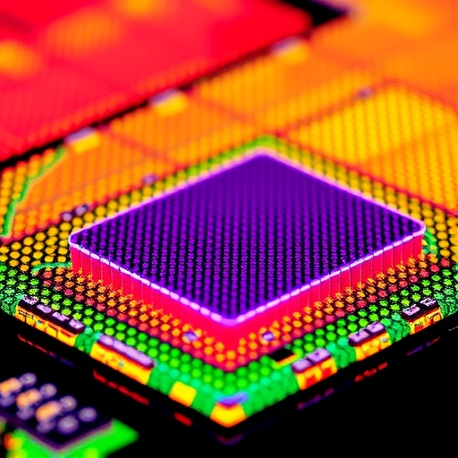
Optoelectronic imaging is rapidly shrinking while gaining capability, a shift driven by needs in autonomous navigation, portable medical diagnostics, and drone-based inspection. Yet conventional refractive systems—built from cascaded lens assemblies and microlens arrays—struggle to scale down because their spatial footprint consumes valuable volume. That limitation makes miniaturization difficult to sustain as cameras and sensors move toward compact, high-density form factors.
A promising route is the metasurface, a planar optical element engineered at the nanoscale to control phase, amplitude, and polarization of light. Unlike lenses that rely on spatial phase accumulation, metasurfaces shape wavefronts through subwavelength patterning. This difference can remove key bulk constraints and open the door to imaging modules that are truly thin and lightweight.
In new work from a team led by Prof. Boxiang Song and Prof. Jiang Tang at Huazhong University of Science and Technology (HUST), researchers push metasurfaces toward fully integrated sensing architectures. Their approach merges metasurface optics with photodetectors and image sensors, targeting architectures that can move from separate components toward a unified on-chip platform.
The study outlines a developmental path: beginning with metasurfaces placed in free space, then transitioning to hybrid adhesive mounting, and ultimately aiming for direct monolithic fabrication. Each stage addresses practical integration challenges, but the monolithic endpoint is positioned as the strongest integration frontier.
A core idea is fabricating metasurfaces directly onto active materials so that resonant nanostructures sit in the near-field of the photoelectric depletion region. This proximity is essential: it places the optical resonances where they can interact more effectively with carrier generation and collection processes.
By coupling the metasurface’s structured light fields into the semiconductor near-field, the system can actively break absorption constraints that typically limit efficiency in conventional optical front-ends. As a result, multi-parameter optical information can be converted into electrical signals in a single-shot readout.
The researchers emphasize that their architecture enables multi-dimensional perception without the need for bulky optical stacks. Such capability is especially relevant for fast imaging scenarios where computational delay and mechanical complexity are undesirable.
The article, titled “Integration of metasurface with photodetectors and image sensors: towards ultra-compact, multi-functional and on-chip optoelectronic imaging systems,” was published in Frontiers of Optoelectronics on June 18, 2026.
Article Title: Integration of metasurface with photodetectors and image sensors: towards ultra-compact, multi-functional and on-chip optoelectronic imaging systems
News Publication Date: June 18, 2026
Web References: https://journal.hep.com.cn/foe/EN/10.2738/foe.2026.0036
References: doi:10.2738/foe.2026.0036
Image Credits: HIGHER EDUCATION PRESS
Keywords: metasurface, photodetectors, monolithic integration, on-chip imaging, ultra-compact optoelectronics
Tags: autonomous navigation sensor technologydrone inspection optical systemshybrid mounting of metasurfaces on image sensorsintegrated optoelectronic miniaturizationlightweight and thin optical sensor designMetasurface-based ultracompact imaging sensorsmetasurface-enabled high-density sensor architecturesminiaturized medical diagnostic imaging devicesmonolithic metasurface photodetector integrationnanoscale optical phase control for sensorsnanoscale wavefront shaping for portable imagingon-chip metasurface imaging modules