Credit: by Hong Liu
In contemporary society, the demand for high-bandwidth optical communication, including mobile high-definition videos, autonomous vehicles, remote surgery, telepresence, and interactive 3D virtual reality gaming, is sharply increasing. The electro-optical modulator is the key component for optical fiber communication, which modulates the light signal for loading information through electricity. Lithium niobate (LiNbO3, LN) exhibits a high-performance electro-optic effect and high optical transparency. On the other hand, the ferroelectric domain engineering on LN crystals has been extended from 1D to 2D and 3D. Moreover, considering the device size, reliability, cost, and energy consumption, the photonic integrated circuit (PIC) technology has recently gained signi?cant interest in the rise of the integrated photonics field. Integrated photonics is concerned with the integration of all the key components connected by a waveguide in a single chip (photonic platform) using a single material (monolithic integration) or multi-materials (hybrid integration). Over the past 25 years, integrated lithium niobate photonics have relied almost exclusively on the high-quality lithium niobate thin film on insulator (LNOI) technology and advanced PIC technology for etching nanophotonic waveguides and microphotonic modulators. Lithium niobate has launched a photon revolution as silicon did for electronics. Herein, we review the progress of microstructure engineering and domain engineering of LNOI for integrated lithium niobate photonics, including photonic modulation and nonlinear photonics.
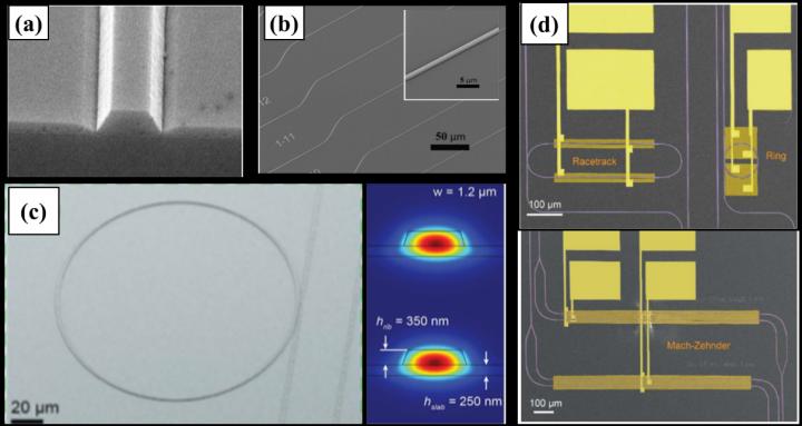
For photonic modulation, both the complementary approaches of microstructure engineering for photonic circuits, i.e., the direct etching of LNOI (monolithic integration) and other photonic materials rib-loaded on LNOI (hybrid integration), are reviewed. The sub-wavelength waveguides with a low propagation loss of 2.7 dB/m as well as an ultra-high Q of 5 × 10⁶ have been fabricated by direct etching on a LNOI platform. Furthermore, The integrated MZI modulator with a small size of several millimeters on a x-cut LNOI exhibited a very high bandwidths of up to 100 GHz. The smart cut method for the preparation of wafer-scale LNOI samples (NanoLN, Jinan Jingzheng Electronics Co., Ltd.) greatly promoted the development of integrated lithium niobate photonics. the substitution of z-cut LN film by a x-cut LN film greatly promoted the integration level of photonic circuits. The channel patterns with electrodes were easily transferred into a x-cut LN film, while the bottom electrode generally occupy the whole plane for a z-cut LN film. Importantly, the gold electrodes can be placed very tightly from the edge of a resonator on a x-cut LN film, which results in strong phase modulation without affecting the Q factor.
In addition, the hybrid integration of photonic materials with a LN film is an effective approach for the integrated photonics, which can avoid the etching of LN. However, no matter the LN film works as top cladding or substrate, the transition loss between the two layers is still a problem for this hybrid waveguide. Though the design of VACs nearly resolved the problem of transition loss, the nanophotonic LN waveguide was still adopted and the waveguide parameters must be precisely controlled for high modulation efficiency and low optical loss. It doesn’t fully reflect strengths of hybrid integration which avoids the etching of LN. Therefore, the approach of hybrid integration still needs further improvement.
High-efficiency, compact, and integration-compatible wavelength converters using optical waveguides involve nonlinear integrated photonics. Generally, photonic microstructures used for frequency conversion are designed based on a stronger mode confinement because the nonlinear effect can significantly enhance inside a small modal volume due to the increased field strength and temporal confinement of the interacting modes. Metasurfaces consisting of nanoantennas are often used for enhanced optical nonlinearities. A nanophotonic LN waveguide patterned with gradient metasurfaces was fabricated to achieve a monotonic increase in SHG power, resulting in a high-efficiency SHG of approximately 1000% W?1 cm?2, which is three orders of magnitude more efficient than the bare LN waveguide. However, the obvious phase mismatch between the interacting waves often results from material dispersion. Therefore, several phase-matching techniques as well as the associated waveguide microstructure engineering have been explored for second harmonic generation (SHG) processes. Recently developed the integrated frequency-conversion devices on PPLN films also involved hybrid and monoclinic approaches. Generally, the phase-matching condition is a critical factor in nonlinear frequency conversion processes. However, the phase-matching-free SHG has been achieved with high-efficiency conversion by the gradient metasurface on an on-chip integrated nonlinear photonic device. This found will promote the development of nonlinear integrated photonics on LNOI. Of course, many integrated nonlinear photonic devices were fabricated by following the phase-matching SHG, especially quasi-phase-matching. The preparation of PPLN film greatly promoted the nonlinear integrated photonics on LNOI, especially the nanophotonic PPLN waveguides which realized a conversion efficiency of up to 4600% W-1 cm-2. In the future, the nanophotonic PPLN waveguides will be applied in quantum technology to develop the integrated quantum technology.
Over the last decade, integrated lithium niobate photonics has rapidly developed and proved invaluable in the development of future optical communication and quantum technologies. The large-scale and low-cost manufacturing of integrated photonic devices and systems by mature manufacturing processes will enable new revolutionary applications in optical communication and quantum technologies.
###
Media Contact
Hong Liu
[email protected]
Related Journal Article
http://dx.
