Credit: by Jiayue Han, Meiyu He, Ming Yang, Qi Han, Fang Wang, Fang Zhong, Mengjian Xu, Qing Li, He Zhu, Chongxin Shan, Weida Hu, Xiaoqing Chen, Xinran Wang, Jun Gou, Zhiming…
Since graphene has a low absorption coefficient in the absorption band, researchers generally use graphene as a carrier collection layer, and look for another strong light-absorbing material as the main material for light detection. In order to obtain a photodetecting device with high gain and ultra-high light sensitivity, the graphene photoconductive structure is the main structure for the require of high light responsivity device. However, the existing graphene-based phototransistors mainly use single-layer or single-component organic and inorganic materials as the light absorption enhancement layer of the graphene photoconductive device. This structure suffer low the exciton dissociation efficiency in single light absorption layer. For the lack of an effective dissociation built-in electric field in the vertical direction this structure only utilizes the weak electric field between the graphene and the light-absorbing layer to dissociate excition. This type of device often loses a large amount of light energy.
Traditional optoelectronic devices have always focused on the modulation of the gate voltage. Compared with electrical modulation, the space of development and application in optical modulation is vast. In recent years, light modulation devices have received widespread attention. For example, in previous work, researchers from the Chinese Academy of Sciences used ultraviolet light modulation to achieve input light amplification on porous silver/titanium oxide heterojunctions [Advanced Functional Materials 28 (2018) :1802288]. In addition, researchers from the Shanghai Institute of Technical Physics used visible light-assisted processing on InAs nanowire devices to extend the detection wavelength up to 3133 nm [Nano Letters 16 (2016): 6416-6424]. Generally speaking, optical modulation devices are different from ordinary optoelectronic devices. Such devices need to have different types of optical responses in two wavebands. Therefore, two uncorrelated light responses are required, one acts as modulation light and the other as the input light source.
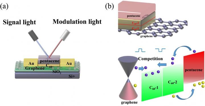
In a new paper published in Light Science & Application, a team of scientists, Professor Jun Wang from School of Optoelectronic Science and Engineering, University of Electronic Science and Technology of China; Shanghai Institute of Technical Physics, Chinese Academy of Science; School of Electronic Science and Engineering, Nanjing University, and co-workers have developed to utilize light modulation for controlling the modulation of photocurrent speed, photocurrent value, and logical direction in the graphene/organic heterojunction sandwich structure. They employed the graphene photoconductive device structure for light modulation with the bi-layer structure of the organic small molecule onto the graphene, relying on the effective exciton thickness limitation of the intermediate organic transport layer. And in the device of the thick intermediate transport layer, the logic reversal of the optical original signal is realized under modulation. And under the optimization of optical modulation, the original optical signal responsivity can also be greatly improved.
Based on the previous work of the bidirectional photocurrent response (negative response at 405-650 nm and positive response at 808-1550 nm) generated by the graphene/C60/pentacene sandwich photoconductive device, two intermodulation of bands are formed. Since the response forms of the two responses are completely different, the photocurrent modulation effects in different situations can be operated through light modulation. The main negative response in the visible light band is produced by C60/pentacene, while the near-infrared positive response is mainly produced by graphene and C60. Graphene is mainly doped by water vapor and oxygen in the room temperature atmosphere and resulting in hole-dominated. The photogenerated electrons generated from C60/pentacene will inject into the graphene channel with the built-in electric field giving a negative response. The photogenerated electrons generated from heterojunction graphene/C60 will inject into C60, which will deepen the holes doping in graphene. These two opposite light doping effects provide favorable conditions for the mutual modulation of these two bands. These scientists summarize the functions of their phototransistor:
‘The photoelectric device we designed can realize 3 different modulations: 1. It can realize the modulation of the photocurrent magnitude. 2. It can realize the modulation of the response speed. 3. The polarity of the photocurrent can be modulated.’
‘Using these, we can realize all-optical input optical modulation devices with excellent performance in the future, which will provide a reference for the preparation and design of replacement electrical modulation functional devices in the future.’ they added.
###
Media Contact
Jun Wang
[email protected]
Related Journal Article
http://dx.


