Credit: University of Rostock
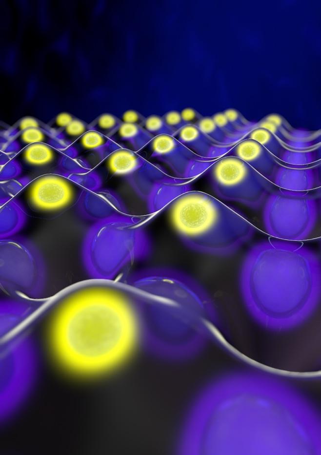
The researchers used powerful laser flashes to irradiate thin, films of crystalline materials. These laser pulses drove crystal electrons into a fast wiggling motion. As the electrons bounced off with the surrounding electrons, they emitted radiation in the extreme ultraviolet part of the spectrum. By analyzing the properties of this radiation, the researchers composed pictures that illustrate how the electron cloud is distributed among atoms in the crystal lattice of solids with a resolution of a few tens of picometers which is a billionth of a millimeter. The experiments pave the way towards developing a new class of laser-based microscopes that could allow physicists, chemists, and material scientists to peer into the details of the microcosm with unprecedented resolution and to deeply understand and eventually control the chemical and the electronic properties of materials. (Nature, July 1 2020)
For decades scientists have used flashes of laser light to understand the inner workings of the microcosm. Such lasers flashes can now track ultrafast microscopic processes inside solids. Still they cannot spatially resolve electrons, that is, to see how electrons occupy the minute space among atoms in crystals, and how they form the chemical bonds that hold atoms together. The reason is long known. It was discovered by Abbe more than a century back. Visible light can only discern objects commensurable in size to its wavelength which is approximately few hundreds of nanometers. But to see electrons, the microscopes have to increase their magnification power by a few thousand times.
To overcome this limitation, Goulielmakis and coworkers took a different path. They developed a microscope that works with powerful laser pulses. They dubbed their device as the Light Picoscope. “A powerful laser pulse can force electrons inside crystalline materials to become the photographers of the space around them.” When the laser pulse penetrates inside the crystal, it can grab an electron and drive it into a fast- wiggling motion. “As the electron moves, it feels the space around it, just like your car feels the uneven surface of a bumpy road,” said Harshit Lakhotia, a researcher of the group. When the laser-driven electrons cross a bump made by other electrons or atoms, it decelerates and emits radiation at a frequency much higher than that of the lasers. “By recording and analyzing the properties of this radiation, we can deduce the shape of these minute bumps, and we can draw pictures that show where the electron density in the crystal is high or low,” said Hee-Yong Kim, a doctorate researcher in Extreme Photonics Labs. “Laser Picoscopy combines the capability of peering into the bulk of materials, like x-rays, and that of probing valence electrons. The latter is possible by scanning tunneling microscopes but only on surfaces.”
“With a microscope capable of probing, the valence electron density we may soon be able to benchmark the performance of computational solid-state physics tools,” said Sheng Meng, from the Institute of Physics, Beijing, and a theoretical solid-state physicist in the research team. “We can optimize modern, state-of-the-art models to predict the properties of materials with ever finer detail. This is an exciting aspect that laser picoscopy brings in,” he continues.
Now the researchers are working on developing the technique further. They plan to probe electrons in three dimensions and further benchmark the method with a broad range of materials including 2-D and topological materials. “Because laser picoscopy can be readily combined with time-resolved laser techniques, it may soon become possible to record real movies of electrons in materials. This is a long-sought goal in ultrafast sciences and microscopies of matter” Goulielmakis concludes.
###
Media Contact
Prof. Dr. Eleftherios Goulielmakis
[email protected]
Related Journal Article
http://dx.
