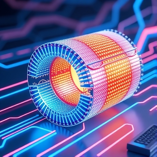
KAIST’s “Oxygen Tunnel” Could Make 3D AI Memory Faster, More Reliable and More Energy Efficient
As artificial intelligence systems become more powerful, the movement of data between processors and memory is emerging as one of the largest obstacles to performance. Modern AI workloads require enormous volumes of information to be transferred rapidly, yet conventional memory technologies struggle to keep up without consuming substantial energy. A research team at the Korea Advanced Institute of Science and Technology, or KAIST, has now developed a device structure designed to address one of the most persistent problems in three-dimensional memory: instability in vertically stacked semiconductor channels. By controlling the movement of oxygen at the nanoscale, the researchers have created an “oxygen-tunnel” architecture that could improve the speed, endurance and power efficiency of future AI chips.
The work focuses on oxide vertical channel transistors, or VCTs, a promising technology for increasing memory density beyond the limits of conventional planar designs. In a vertical channel device, electrical current flows through a semiconductor channel oriented vertically rather than horizontally. This architecture allows memory cells and transistors to be stacked in multiple layers, creating a three-dimensional structure that can hold more computing and storage elements within a smaller footprint. Such designs are particularly attractive for compute-in-memory systems, which perform calculations directly where data are stored instead of repeatedly moving information between separate memory and processor units.
The central challenge lies in the behavior of oxygen inside oxide semiconductors. These materials can contain oxygen vacancies, which are sites where oxygen atoms are missing from the crystal or amorphous structure. Although these vacancies may be useful in carefully controlled amounts, excessive or unstable concentrations can create unwanted electronic states, alter the transistor’s threshold voltage and increase leakage or variability. Over time, such defects can cause the electrical properties of the channel to drift, undermining the reliability required for memory and AI hardware. Supplying additional oxygen can compensate for these vacancies, but the solution creates another problem: oxygen may continue migrating beyond the channel and oxidize the nearby metal electrode.
That oxidation at the electrode interface can increase contact resistance, making it more difficult for current to enter and leave the transistor. The result is a fundamental materials trade-off. The semiconductor channel needs a controlled supply of oxygen to remain electrically stable, while the electrode must be shielded from the same oxygen to preserve a low-resistance connection. Conventional interlayer dielectric materials do not provide sufficient directional control, allowing oxygen to diffuse through regions where it can damage the device. KAIST researchers therefore designed a multilayer structure intended to guide oxygen toward the channel and block its movement toward the electrode.
The new structure consists of alternating layers of silicon nitride, silicon dioxide and silicon nitride, abbreviated as SiN/SiO₂/SiN. Rather than acting as a simple insulating barrier, this stack functions as a selective oxygen pathway. The researchers engineered the layers so that oxygen released from the interlayer dielectric could reach the oxide semiconductor, where it helps compensate oxygen vacancies, while its diffusion toward the metal contact was suppressed. The concept resembles a microscopic tunnel with a preferred direction of travel. By regulating the local chemical environment around the channel, the oxygen-tunnel architecture improves semiconductor stability without sacrificing the electrical quality of the electrode interface.
The researchers fabricated indium tin oxide vertical channel transistors incorporating the new structure and examined them using cross-sectional transmission electron microscopy. The imaging confirmed the formation of the intended SiN/SiO₂/SiN stack and showed a well-defined hole profile in the fabricated device. This structural evidence was important because the performance of vertically integrated transistors depends heavily on the precision of nanoscale layers and interfaces. Even small defects, irregularities or unintended diffusion paths can cause large changes in resistance, switching behavior and long-term reliability when thousands or millions of devices are combined in a memory array.
According to KAIST, the oxygen-tunnel transistors achieved high current density while also demonstrating strong data-retention characteristics. The devices maintained their performance during more than ten million cycles of severe electrical stress testing, with the threshold voltage shift remaining below 50 millivolts. Threshold voltage is the gate voltage required to switch a transistor into conduction, and changes in this value can cause a memory cell to be misread or an analog computation to become inaccurate. Limiting the shift to such a small value after repeated operation indicates that the new structure can withstand demanding workloads without the rapid electrical drift that has hindered oxide-based vertical devices.
The potential significance extends beyond memory density. In compute-in-memory hardware, transistors can be used not only to store information but also to perform operations such as multiplication and accumulation, which are fundamental to neural-network processing. These systems can reduce the energy lost when data travel back and forth between memory and a separate processor. The KAIST team evaluated the technology in combination with conventional silicon complementary metal-oxide-semiconductor circuitry and reported results suggesting that the oxide platform could improve the performance of monolithic three-dimensional compute-in-memory systems. Such integration could allow high-density memory layers to be placed directly above logic circuits, shortening interconnects and increasing the number of operations performed per unit of area.
The research was led by Hyeonho Gu, with Yongwoo Lee, Haksoon Jung and Jimin Kwon serving as corresponding authors, in collaboration with scientists from UNIST, Yonsei University, the Korea Research Institute of Chemical Technology, Seoul National University and other Korean institutions. Published in Advanced Functional Materials, the study presents oxygen migration control as a new route to solving reliability problems in vertically stacked oxide electronics. The paper, titled “Oxygen-Tunnel Indium Tin Oxide Vertical Channel Transistors with Enhanced Current Density and Reliability for Monolithic 3D Compute-In-Memory Systems,” was also selected as a Front Cover article. If the approach can be scaled to large arrays and integrated into manufacturing processes, it could help advance the ultra-low-power AI memory systems needed for increasingly data-intensive applications.
Subject of Research: Oxygen-tunnel indium tin oxide vertical channel transistors for reliable, high-density memory and monolithic 3D compute-in-memory systems.
Article Title: Oxygen-Tunnel Indium Tin Oxide Vertical Channel Transistors with Enhanced Current Density and Reliability for Monolithic 3D Compute-In-Memory Systems
Web References: https://doi.org/10.1002/adfm.202531989
References: Advanced Functional Materials, DOI: 10.1002/adfm.202531989
Image Credits: KAIST
Keywords
AI chips, three-dimensional memory, compute-in-memory, oxide semiconductors, vertical channel transistors, indium tin oxide, oxygen vacancies, oxygen migration, silicon nitride, silicon dioxide, semiconductor reliability, low-power computing
Tags: 3D vertical channel transistorsAI chip memoryenergy-efficient AI hardwarehigh-density 3D memory technologyimproved AI memory speed and reliabilityKAIST AI hardware innovationnanoscale oxygen control in semiconductorsovercoming 3D memory instabilityoxide VCTs for AIoxygen tunnel architecturepower-efficient 3D memory devicesstacked semiconductor memory architecture