


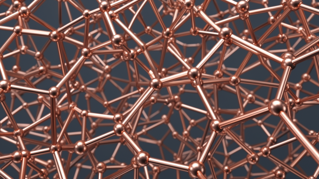
Researchers at GSI Helmholtzzentrum für Schwerionenforschung in Darmstadt, Germany, have demonstrated a robust method for fabricating three-dimensional nanowire networks using ion track nanotechnology. Published in EPJ Techniques and Instrumentation, the study details how swift heavy ions can create precise templates in polymer foils, which are subsequently filled with metals and semiconductors to form stable, interconnected nanostructures. These networks combine the mechanical stability of macroscopic samples with the unique size-dependent properties of individual nanowires, offering a new platform for applications in photoelectrochemistry and thermoelectrics.
The fabrication process begins with the irradiation of polycarbonate foils, specifically Makrofol N, with high-energy heavy ions such as gold or bismuth. The ions are accelerated to specific energies of up to 11.4 MeV per nucleon at the UNILAC accelerator facility. As these ions pass through the polymer, they deposit enormous energy densities along their trajectories, creating long, nanoscopic damage trails known as ion tracks. The penetration depth of these beams allows for the exposure of foil stacks with thicknesses ranging from approximately 6 to 100 micrometers, providing the necessary volume for three-dimensional growth.
To create the network geometry, the polymer foils are irradiated sequentially from four different directions, with each direction separated by 90 degrees. During each step, the foil is tilted at a 45-degree angle relative to the incoming ion beam. This multi-angle irradiation results in a complex lattice of intersecting ion tracks. Following irradiation, the foils are exposed to ultraviolet light at 312 nanometers, a process that narrows the distribution of pore sizes. Subsequent chemical etching in a 6 molar sodium hydroxide solution at 50 degrees Celsius selectively dissolves the ion tracks, enlarging them into open, cylindrical nanochannels with diameters that grow at a radial rate of 10 to 12 nanometers per minute.
Once the template is prepared, a conductive layer, typically a 100-nanometer thin gold film, is sputtered onto one side of the membrane to serve as a working electrode. The template is then placed in a three-electrode electrochemical cell, where electrodeposition fills the nanochannels with the desired material. By controlling the applied potential and the duration of the deposition, researchers can precisely adjust the length, composition, and crystallographic orientation of the resulting nanowires. After the metal is deposited, the polymer matrix is dissolved in dichloromethane, leaving behind a freestanding, three-dimensional network of nanowires that spans cross-sectional areas of up to several square centimeters.
The resulting networks exhibit high mechanical stability due to the numerous junctions between adjacent nanowires. These interconnections allow the wires to support one another, ensuring that electrical or thermal transport can continue even if individual wires break. The surface area of these structures is substantial, reaching up to 250 square centimeters on a 1 cm² planar surface. This high surface-to-volume ratio is particularly advantageous for electrochemical applications, as it maximizes the interface between the electrode and the electrolyte, facilitating efficient charge carrier transport and reducing recombination losses.
In the field of photoelectrochemistry, the study highlights the use of zinc oxide (ZnO) nanowire networks as photoanodes for water splitting. When illuminated with an arc lamp source calibrated at AM 1.5, the ZnO networks generated significantly higher photocurrents than flat ZnO thin films. At a bias voltage of 1.5 volts versus the reversible hydrogen electrode, the networks produced a photocurrent density of 0.1 mA/cm², compared to 0.02 mA/cm² for the thin films. This fivefold increase is attributed to the one-dimensional geometry of the nanowires, which enhances light absorption and charge carrier transport to the electrolyte interface.
To protect the zinc oxide from photocorrosion, a 20-nanometer thick layer of titanium dioxide (TiO₂) was applied via atomic layer deposition. The TiO₂-coated networks showed even higher performance, generating 0.35 mA/cm² at the same bias voltage. Scanning electron microscopy images revealed that while uncoated nanowires decayed and recrystallized after one hour of reaction, the TiO₂-coated networks remained largely intact after three hours. The study also demonstrated that increasing the nanowire diameter and density further boosted the generated photocurrent, confirming that the network structure serves as an excellent model system for investigating geometrical factors in photoelectrochemical water splitting.
The research also explored the thermoelectric properties of bismuth (Bi) and antimony (Sb) nanowire networks. The thermoelectric efficiency of a material is described by the dimensionless figure-of-merit, ZT, which depends on the Seebeck coefficient, electrical conductivity, and thermal conductivity. While commercial thermoelectric materials typically exhibit ZT values around 1, the study suggests that nanowire networks could potentially improve this efficiency by decoupling electrical and thermal transport. The mean free paths of charge carriers and phonons in Bi and Sb are on the order of 100 nanometers, meaning that size effects become significant at the dimensions of these nanowires.
Measurements of Sb nanowire networks with diameters ranging from 30 to 140 nanometers showed that the electrical resistivity is dominated by scattering at the nanowire surfaces and grain boundaries. The Seebeck coefficient for these networks was measured at 20 to 25 microvolts per kelvin, which is lower than the maximum value of 47 microvolts per kelvin observed in bulk Sb but comparable to values for other crystal orientations. The thermal conductivity of the Sb networks was found to be significantly lower than that of bulk Sb, measuring approximately 0.3 to 0.4 watts per meter-kelvin compared to 24 watts per meter-kelvin for the bulk material. This suppression of thermal conductivity, combined with a Seebeck coefficient similar to bulk material, suggests that the thermoelectric efficiency ZT is likely increased in the network structures.
For bismuth nanowire networks, the Seebeck coefficient at room temperature decreased as the wire diameter decreased, a trend attributed to the limitation of the charge carrier mean free path and the influence of surface states. A notable finding was the change in the sign of the Seebeck coefficient at lower temperatures, a behavior that was not observed in the antimony networks. The temperature at which this sign change occurred shifted to higher values as the nanowire diameter decreased. This phenomenon is consistent with theoretical predictions for bismuth nanowires oriented along the bisectrix axis, where the mobility of holes and electrons depends differently on diameter and temperature.
The study emphasizes that these 3D nanowire networks are not merely collections of individual wires but are integrated systems with unique collective properties. The ability to control the geometry, composition, and crystallographic properties of the networks provides a versatile platform for developing novel devices. The mechanical stability of the networks, derived from their interconnected structure, allows them to be handled as macroscopic samples, which is a significant advantage for practical applications in sensing, catalysis, and energy conversion.
While the results are promising, the authors note that absolute values of electrical resistance must be measured in future work to fully quantify the thermoelectric performance of these networks. The current study provides a strong foundation for understanding how size and geometry influence transport properties in semimetals and semiconductors. The combination of ion-track nanotechnology and electroplating offers a scalable and precise method for creating these tailored nanostructures, opening new avenues for interdisciplinary research in materials science and nanotechnology.
This work underscores the potential of accelerator-based facilities to drive innovation in nanotechnology. By leveraging the unique capabilities of swift heavy ions, researchers can create complex, three-dimensional architectures that were previously difficult to fabricate. The study provides a comprehensive overview of the synthesis and characterization of these networks, highlighting their suitability for both fundamental research and practical applications in the fields of photoelectrochemistry and thermoelectrics.
Subject of Research: Fabrication and application of 3D nanowire networks via ion track nanotechnology
Article Title: Three-dimensional nanowire networks fabricated by ion track nanotechnology and their applications
Article References: Wagner, M. F. P., Voss, K. O., Trautmann, C., & Toimil-Molares, M. E. (2023). Three-dimensional nanowire networks fabricated by ion track nanotechnology and their applications. EPJ Techniques and Instrumentation, 10(1), Article 2. https://doi.org/10.1140/epjti/s40485-023-00090-9
Image Credits: AI Generated
DOI: 10.1140/epjti/s40485-023-00090-9
Keywords: nanotechnology, ion tracks, nanowires, photoelectrochemistry, thermoelectrics, materials science, electrodeposition, GSI, semiconductors, bismuth, zinc oxide, Three-dimensional
News Source: Denise Maddox. (November 12, 2026). Ion Track Technology Creates Stable 3D Nanowire Networks. Scienmag.