In a remarkable leap forward for semiconductor technology, researchers have unveiled an innovative method for growing gallium-based (Ga-based) semiconductor thin films that promises to revolutionize optoelectronics, flexible devices, and neuromorphic computing. Traditional semiconductor film fabrication methods, relying heavily on post-synthesis assembly and epitaxial growth, often struggle with high complexity and restricted substrate compatibility. These limitations hinder progress toward the multifunctional needs of burgeoning Internet of Things ecosystems and next-generation wearable technologies. Now, an international research team, led by Professor Zai-xing Yang, has pioneered what they term an “induced fit” growth process — a substrate-independent, scalable approach that could chart new directions in semiconductor applications.
The induced fit growth mechanism takes inspiration from molecular biology, where enzymes undergo conformational changes upon substrate binding to facilitate biochemical reactions. Analogously, this method exploits a Ga-rich surface on a freshly exfoliated GaOx film that encourages the deposition of vaporized atoms, catalyzing uniform nucleation and compact thin-film formation. This strategy circumvents the typical restrictions imposed by lattice mismatch between the film and substrate, enabling the growth of high-quality films such as GaSb, GaSe, GaAs, and GaAsSb across diverse functional substrates.
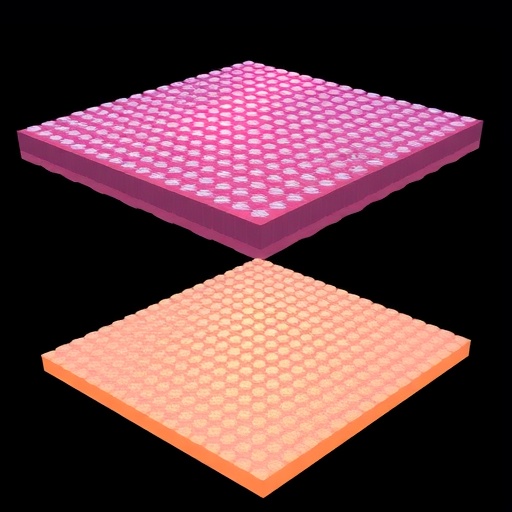
The resulting Ga-based semiconductor thin films exhibit exceptional uniformity with compact, defect-minimized morphologies demonstrated over centimeter-scale dimensions. Scanning electron microscopy reveals a densely packed surface free of cracks or discontinuities, indicative of excellent film coherence. This level of control in film morphology and thickness tuning is critical for downstream integration into flexible, transparent optoelectronic circuits and sensor arrays, offering pathways to mass-producible, robust devices.
Performance-wise, the induced fit-grown films illustrate an impressive p-type conduction behavior when utilized as active channels in thin film transistors (TFTs). These devices showcase high current densities and enhanced hole mobility — improvements vital for achieving rapid switching speeds and low power consumption in electronic circuits. Crucially, transistor performance improves with prolonged growth duration, underscoring the growth process’s ability to optimize charge transport pathways and reduce trap states within the semiconductor matrix.
Beyond conventional transistor applications, the team’s work demonstrates that these semiconductor films can convincingly emulate synaptic functionalities inherent to biological neural networks. The TFTs mimic spike timing-dependent plasticity, a dynamic synaptic behavior fundamental to learning and memory in biological systems. Such neuromorphic properties position these Ga-based thin films as promising candidates for brain-inspired computing technologies, which seek to transcend traditional von Neumann architectures with efficient, parallel signal processing analogs.
The research also extends to optoelectronic applications, where the films’ broadband photodetection capabilities have been tested. Photodetectors fabricated from the films effectively respond across a wide spectral range, from visible to infrared wavelengths, with spectacular photoresponse uniformity across device arrays. This broadband sensitivity, coupled with the films’ innate flexibility, enables the construction of adaptable imaging arrays — highlighted by a 5 × 5 pixel sensor matrix delivering precise and uniform imaging performance. Such devices hold extraordinary promise for flexible, wearable photodetectors and imaging systems in ambient, indoor, and harsh environmental conditions.
A particularly compelling feature of this growth approach is its versatility to produce films on a broad spectrum of substrates without the constraints typically imposed by lattice parameters. This substrate independence facilitates integration onto flexible polymers, transparent electrodes, and even biologically compatible platforms, vastly broadening the design space for multifunctional optoelectronic systems. This capability aligns seamlessly with the increasing demand for wearable, implantable electronics and the emergent Internet of Things landscape where device conformity to irregular surfaces is paramount.
Microscale patterning techniques have further enhanced the utility of these films, enabling their deployment in large-scale optoelectronic device arrays with intricate spatial resolution. The compatibility of the induced fit growth method with microfabrication processes suggests that scalable manufacturing of Ga-based semiconductor thin films can coalesce with existing CMOS-friendly workflows, accelerating their transition from laboratory prototypes to commercial viability.
Professor Zai-xing Yang and colleagues emphasize that this technique marks a significant departure from traditional thin film growth paradigms, laying down a universal platform that democratizes access to high-quality semiconductor films across diverse substrates and applications. They highlight the technology’s potential to spearhead innovations in flexible electronics, neuromorphic devices, and multifunctional optoelectronics, precisely addressing the scaling and multifunctionality requirements of next-generation devices.
Their visionary outlook anticipates that the induced fit growth mechanism will accelerate development timelines for wearable and implantable technologies by reliably delivering semiconductor films that seamlessly combine electronic performance, mechanical flexibility, transparency, and synaptic-like behavior. This multi-property synergy represents a vital step toward realizing smart, adaptive electronics embedded within everyday environments and the human body.
In conclusion, the development of an induced fit growth technique for Ga-based semiconductor thin films represents a watershed moment for materials science and device engineering alike. By circumventing the inherent challenges of conventional film growth, this substrate-agnostic, biologically inspired approach unlocks pathways to multifunctional, high-performance films poised to transform optoelectronics, neuromorphic computing, and beyond. As these films progress through further optimization and integration, their poised impact on wearable, implantable, and flexible electronics could well redefine the technological landscape of the near future.
Subject of Research: Induced fit growth of gallium-based semiconductor thin films for multifunctional optoelectronics and neuromorphic devices
Article Title: Induced fit growth of Ga-based semiconductor thin films for brain-inspired electronics and optoelectronics
News Publication Date: Not explicitly stated in the provided content
Web References: DOI 10.1038/s41377-025-02096-2
References: Zai-xing Yang et al., Light: Science & Applications
Image Credits: Zai-xing Yang et al.
Tags: brain-inspired electronics materialsflexible optoelectronic devicesgallium-based thin film fabricationGaOx film surface catalysisinduced fit growth method for semiconductorslattice mismatch overcoming strategiesmultifunctional IoT semiconductor applicationsneuromorphic computing materialsnext-generation wearable semiconductor filmsscalable thin film deposition techniquessubstrate-independent semiconductor growthuniform GaSb GaSe GaAs thin films

