Credit: The University of Manchester
A team of researchers based in Manchester, the Netherlands, Singapore, Spain, Switzerland and the USA has published a new review on a field of computer device development known as spintronics, which could see graphene used as building block for next-generation electronics.
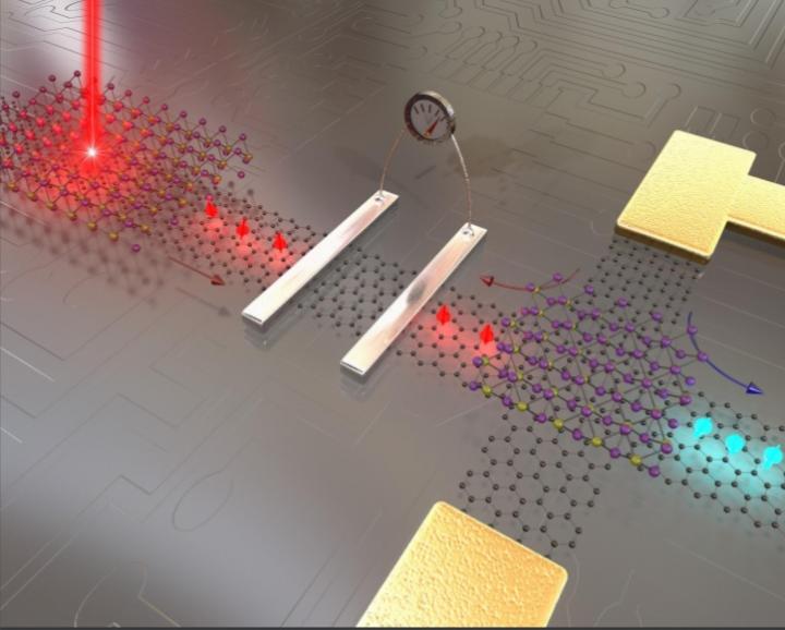
Recent theoretical and experimental advances and phenomena in studies of electronic spin transport in graphene and related two-dimensional (2D) materials have emerged as a fascinating area of research and development.
Spintronics is the combination of electronics and magnetism, at the nanoscale and could lead to next generation high-speed electronics. Spintronic devices are a viable alternative for nanoelectronics beyond Moore’s law, offering higher energy efficiency and lower dissipation as compared to conventional electronics, which relies on charge currents. In principle we could have phones and tablets operating with spin-based transistors and memories.
As published in APS Journal Review of Modern Physics, the review focuses on the new perspectives provided by heterostructures and their emergent phenomena, including proximity-enabled spin-orbit effects, coupling spin to light, electrical tunability and 2D magnetism.
The average person already encounters spintronics in laptops and PCs, which are already using spintronics in the form of the magnetic sensors in the reading heads of hard disk drives. These sensors are also used in the automotive industry.
Spintronics is a new approach to developing electronics where both memory devices (RAM) and logic devices (transistors) are implemented with the use of ‘spin’, which is the basic property of electrons that cause them to behave like tiny magnets, as well as the electronic charge.
Dr Ivan Vera Marun, Lecturer in Condensed Matter Physics at The University of Manchester said: “The continuous progress in graphene spintronics, and more broadly in 2D heterostructures, has resulted in the efficient creation, transport, and detection of spin information using effects previously inaccessible to graphene alone.
“As efforts on both the fundamental and technological aspects continue, we believe that ballistic spin transport will be realised in 2D heterostructures, even at room temperature. Such transport would enable practical use of the quantum mechanical properties of electron wave functions, bringing spins in 2D materials to the service of future quantum computation approaches.”
Controlled spin transport in graphene and other two-dimensional materials has become increasingly promising for applications in devices. Of particular interest are custom-tailored heterostructures, known as van der Waals heterostructures, that consist of stacks of two-dimensional materials in a precisely controlled order. This review gives an overview of this developing field of graphene spintronics and outlines the experimental and theoretical state of the art.
Billions of spintronics devices such as sensors and memories are already being produced. Every hard disk drive has a magnetic sensor that uses a flow of spins, and magnetic random access memory (MRAM) chips are becoming increasingly popular.
Over the last decade, exciting results have been made in the field of graphene spintronics, evolving to a next generation of studies extending to new two-dimensional (2D) compounds.
Since its isolation in 2004, graphene has opened the door for other 2D materials. Researchers can then use these materials to create stacks of 2D materials called heterostructures. These can be combined with graphene to create new ‘designer materials’ to produce applications originally limited to science fiction.
Professor Francisco Guinea who co-authored the paper said: “The field of spintronics, the properties and manipulation of spins in materials has brought to light a number of novel aspects in the behaviour of solids. The study of fundamental aspects of the motion of spin carrying electrons is one of the most active fields in the physics of condensed matter.”
The identification and characterisation of new quantum materials with non-trivial topological electronic and magnetic properties is being intensively studied worldwide, after the formulation, in 2004 of the concept of topological insulators. Spintronics lies at the core of this search. Because of their purity, strength, and simplicity, two dimensional materials are the best platform where to find these unique topological features which relate quantum physics, electronics, and magnetism.”
Overall, the field of spintronics in graphene and related 2D materials is currently moving towards the demonstration of practical graphene spintronic devices such as coupled nano-oscillators for applications in fields of space communication, high?speed radio links, vehicle radar and interchip communication applications.
Advanced materials is one of The University of Manchester’s research beacons – examples of pioneering discoveries, interdisciplinary collaboration and cross-sector partnerships that are tackling some of the biggest questions facing the planet. #ResearchBeacons
###
Media Contact
Ben Robinson
[email protected]
Original Source
https:/
Related Journal Article
http://dx.


