New compound may replace toxic mercury cadmium telluride and gallium arsenide in near-infrared devices
Credit: NIMS
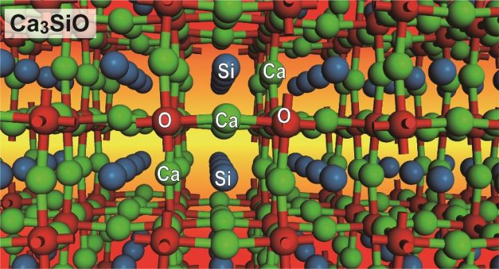
NIMS and the Tokyo Institute of Technology have jointly discovered that the chemical compound Ca3SiO is a direct transition semiconductor, making it a potentially promising infrared LED and infrared detector component. This compound–composed of calcium, silicon and oxygen–is cheap to produce and non-toxic. Many of the existing infrared semiconductors contain toxic chemical elements, such as cadmium and tellurium. Ca3SiO may be used to develop less expensive and safer near-infrared semiconductors.
Infrared wavelengths have been used for many purposes, including optical fiber communications, photovoltaic power generation and night vision devices. Existing semiconductors capable of emitting infrared radiation (i.e., direct transition semiconductors) contain toxic chemical compounds, such as mercury cadmium telluride and gallium arsenide. Infrared semiconductors free of toxic chemical elements are generally incapable of emitting infrared radiation (i.e., indirect transition semiconductors). It is desirable to develop high-performance infrared devices using non-toxic, direct transition semiconductors with a band gap in the infrared range.
Conventionally, the semiconductive properties of materials, such as energy band gap, have been controlled by combining two chemical elements that are located on the left and right side of group IV elements, such as III and V or II and VI. In this conventional strategy, energy band gap becomes narrower by using heavier elements: consequently, this strategy has led to the development of direct transition semiconductors composed of toxic elements, such as mercury cadmium telluride and gallium arsenide. To discover infrared semiconductors free of toxic elements, this research group took an unconventional approach: they focused on crystalline structures in which silicon atoms behave as tetravalent anions rather than their normal tetravalent cation state. The group ultimately chose oxysilicides (e.g., Ca3SiO) and oxygermanides with an inverse perovskite crystalline structure, synthesized them, evaluated their physical properties and conducted theoretical calculations. These processes revealed that these compounds exhibit a very small band gap of approximately 0.9 eV at a wavelength of 1.4 μm, indicating their great potential to serve as direct transition semiconductors. These compounds with a small direct band gap may potentially be effective in absorbing, detecting and emitting long infrared wavelengths even when they are processed into thin films, making them very promising near-infrared semiconductor materials to be used in infrared sources (e.g., LEDs) and detectors.
In future research, we plan to develop high-intensity infrared LEDs and highly sensitive infrared detectors by synthesizing these compounds in the form of large single-crystals, developing thin film growth processes and controlling their physical properties through doping and transforming them into solid solutions. If these efforts bear fruit, toxic chemical elements currently used in existing near-infrared semiconductors may be replaced with non-toxic ones.
###
This project was carried out by a research team consisting of Naoki Ohashi (Director of the Research Center for Functional Materials, NIMS) and Alexander Shluger (Professor, University College London (UCL)). This work was supported by the MEXT Element Strategy Initiative (core research center: Tokodai Institute for Element Strategy) and the JSPS Core-to-Core Program which enabled the NIMS-UCL collaboration.
This research was published in the online version of Inorganic Chemistry, a journal of the American Chemical Society, on December 10, 2020, local time.
Contacts
(Regardins this research)
Naoki Ohashi
Director
Research Center for Functional Materials
National Institute for Materials Science
Tel: +81-29-860-4437
Email: OHASHI.Naoki=nims.go.jp
(Please change “=” to “@”)
Hideya Kumomi
Specially Appointed Professor
Materials Research Center for Element Strategy
Tokyo Institute of Technology
Email: kumomi=mces.titech.ac.jp
(Please change “=” to “@”)
(General information)
Public Rekations Office
Tel: +81-29-859-2026
Fax : +81-29-859-2017
Email : pressrelease=ml.nims.go.jp
(Please change “=” to “@”)
Public Relations Division
General Affairs Department
Tokyo Institute of Technology
Tel: +81-3-5734-2975, Fax: +81-3-5734-3661
Email: media=jim.titech.ac.jp
(Please change “=” to “@”)
Media Contact
Yasufumi Nakamichi
[email protected]
Original Source
https:/
Related Journal Article
http://dx.


