Compact, CMOS compatible on-chip photon sources have attracted much attention to the scientific community and the semiconductor industry. As the transistor’s feature size is continuously scaling down, also the integration density and switching speed in integrated electronic circuits increases exponentially. This leads to an increasingly large power dissipation from electrical connections between circuit elements. Optical (photonic) interconnects and their core element — the on-chip photon source, represent a promising alternative to circumvent this limitation. However, the most promising state-of-the-art on-chip photon sources typically feature a micrometer-scale size — 1000 times larger than transistors and prevent large-scale integration. Memristors, with active areas in the nanometer or even atomic scale, could be advantageously merged with optical functions to circumvent this limitation while providing versatile functionalities.
Credit: by Bojun Cheng, Till-Maurice Zellweger, Konstantin Malchow, Xinzhi Zhang, Mila Lewerenz, Elias Passerini, Jan Aeschlimann, Ueli Koch, Mathieu Luisier, Alexandros Emboras, Alexandre Bouhelier and Juerg Leuthold
Compact, CMOS compatible on-chip photon sources have attracted much attention to the scientific community and the semiconductor industry. As the transistor’s feature size is continuously scaling down, also the integration density and switching speed in integrated electronic circuits increases exponentially. This leads to an increasingly large power dissipation from electrical connections between circuit elements. Optical (photonic) interconnects and their core element — the on-chip photon source, represent a promising alternative to circumvent this limitation. However, the most promising state-of-the-art on-chip photon sources typically feature a micrometer-scale size — 1000 times larger than transistors and prevent large-scale integration. Memristors, with active areas in the nanometer or even atomic scale, could be advantageously merged with optical functions to circumvent this limitation while providing versatile functionalities.
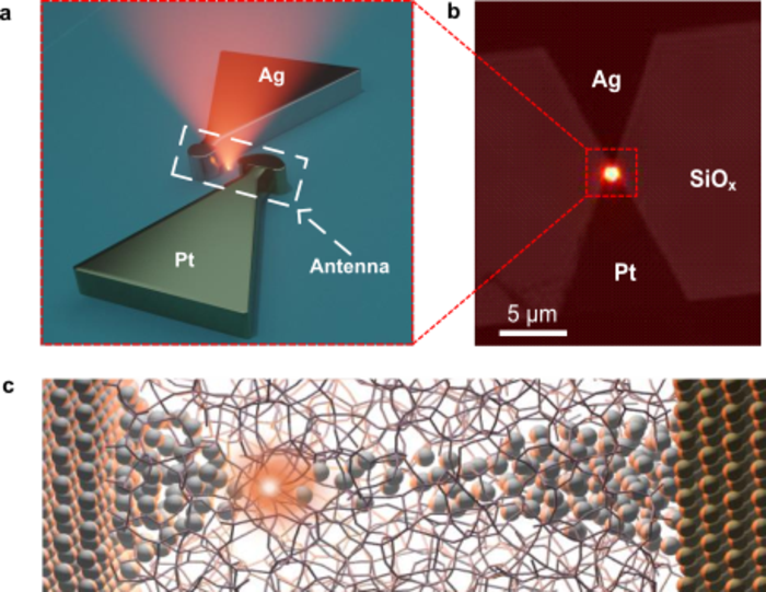
In a recent paper published in Light Science & Application, researchers from ETH Zurich and the University of Burgundy demonstrate an atomic scale memristors capable of emitting photons during resistive switching. This “Atomic Photon Source”, as it is referred to in the paper, consists of a planar Ag/amorphous SiOx/Pt junction with specially engineered electrodes forming optical antennas to enhance the emission efficiency greatly. An illustration of the device structure is depicted in Figure 1a. As shown in Figure 1b, the light emission from the “Atomic Photon Source” can be detected by a CCD camera. As illustrated in Figure 1c, light is emitted during the forming of an electrical connection between the two electrodes, which is comprised of silver atoms that gather up to form a metallic filament.
The researchers further give an explanation on the origin of the light emission in the “Atomic Photon Source”. With a range of experiments, they demonstrate that the light emission stems from an atomic rearrangement of the amorphous SiOx caused by the resistive switching. The atomic composition is locally altered, forming luminescent sites. These sites are then electrically excited and emit photons by a radiative relaxation process.
Due to its compact footprint and CMOS compatible fabrication, this “Atomic Photon Source” could potentially trigger a new conceptual paradigm for devices operating at the atomic level with electrical and optical functionalities embedded on the same nanoscale component. As such, it solves the size mismatch between the current micrometer-sized state art on-chip photon sources and nanometer-sized electrical devices.
Memristors are an emerging category of devices operating in the nanometer scale regime, relying on a different set of atomic scale effects that allow tuning the resistance value of the devices to a desired value. In the case of electro-chemical metallization memories (ECM), the type of memristors investigated by the researchers, the devices consist of simple and CMOS-friendly asymmetric metal-insulator-metal stack. Upon applying a voltage, an active metal atom is oxidized to ions, wanders along the electrical field through the insulator to the passive electrode, and eventually forms a nanometer-sized conductive metallic filament. This process can be reversed and repeated, and data could be stored as the resistance between the electrodes (resistance state). Besides high-density memories, memristors currently receive much attention to their applications where they excel compared to CMOS technology such as neuromorphic and in-memory computing. Interestingly, memristors can also be advantageously merged with optical functions: memristively controlled optical switches and photodetectors have been introduced. Yet, so far, the photonic operation of a memristor relies on external or co-integrated photon sources.
Journal
Light Science & Applications
DOI
10.1038/s41377-022-00766-z


