Credit: POSTECH
As we enter the era of superintelligence and hyper-connected Fourth Industrial Revolution, the importance of high-density and high-performance memory is greater than ever. Currently, the most widely used NAND flash memory has issues of high power consumption, slow operation speed, and vulnerability to repetitive use since it relies on the charge trap effect to store information. To this, a POSTECH research team has recently demonstrated a ferroelectric memory that exceedingly surpasses the performance of the conventional flash memory in terms of operation speed, power consumption, and device reliability.
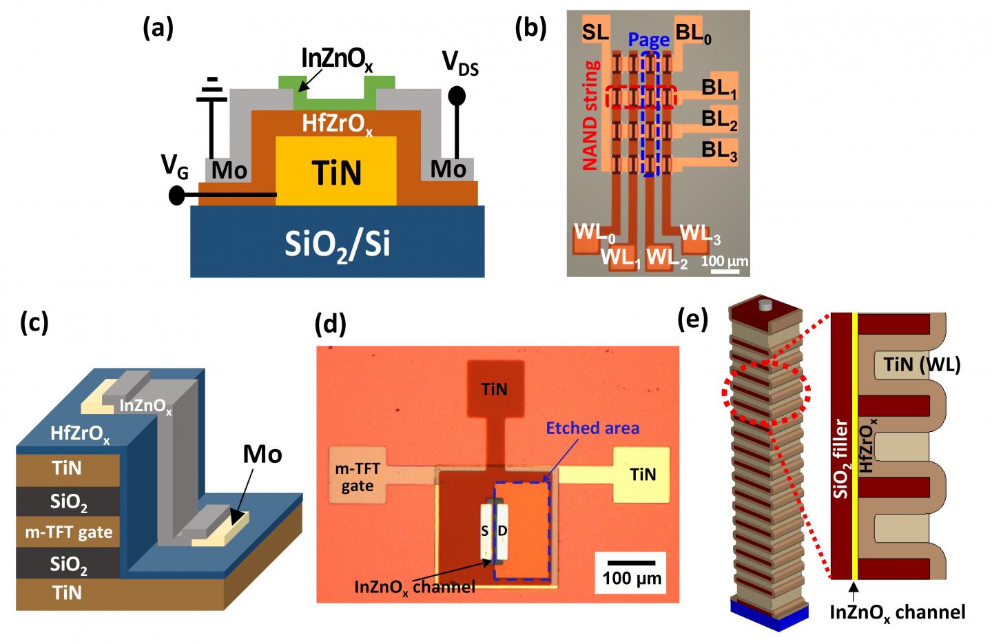
A POSTECH research team – led by Professor Jang-Sik Lee, and Ph.D. candidates Min-Kyu Kim and Ik-Jyae Kim of the Department of Materials Science and Engineering – has demonstrated a unique strategy to fabricate a ferroelectric memory by applying hafnia-based ferroelectrics and oxide semiconductors. This approach yields memory performance that could be achieved neither by the conventional flash memory nor by the previous perovskite ferroelectric memories. Device simulations have confirmed that this strategy can realize ultrahigh-density 3D memory integration.
The ferroelectric memory has gained attention so far for its potential to operate at higher speed with lower power consumption compared to the conventional flash memory. But its commercialization has been deterred due to the high processing temperature, difficulty in scaling, and non-compatibility with the conventional semiconductor processes.
The research team tackled these issues by using the hafnia-based ferroelectrics and oxide semiconductors. The new material and structure ensure low power consumption and high speed; achieve high stability by using oxide semiconductors as channel material to lower the process temperature and suppress the formation of the unwanted interfacial layer. As a result, the researchers confirmed that the fabricated device can operate at a voltage four times lower than that of the conventional flash memory at a speed several hundred times faster and remain stable even when repeatedly used more than 100 million times. In particular, a ferroelectric material and an oxide semiconductor were stacked by an atomic layer deposition to secure a processing technology suitable for manufacturing 3D devices. The team had proposed that high-performance devices can be manufactured under 400°C with much simpler process than that of the conventional flash memory device.
“We have developed the core technology to realize the next-generation of highly integrated and high-performance memory that overcomes the limitations of the conventional 3D NAND flash memory,” remarked Professor Jang-Sik Lee who led the study. He added, “This technology is not only applicable to next-generation memory devices, but also to ultra-low-power and ultrafast highly-integrated universal memory and in-memory computing that are vital to industries like AI and self-driving cars in the future.”
###
Recently published in Science Advances, this research was conducted with the support from Samsung Electronics.
Media Contact
Jinyoung Huh
[email protected]
Original Source
http://postech.
Related Journal Article
http://dx.


