Credit: Ranjit Pati/Michigan Tech
The electron is one of the fundamental particles in nature we read about in school. Its behavior holds clues to new ways to store digital data.
In a study published in Nano Letters, physicists from Michigan Technological University explore alternative materials to improve capacity and shrink the size of digital data storage technologies. Ranjit Pati, professor of physics at Michigan Tech, led the study and explains the physics behind his team’s new nanowire design.
“Thanks to a property called spin, electrons behave like tiny magnets,” Pati said. “Similar to how a bar magnet’s magnetization is dipolar, pointing from south to north, the electrons in a material have magnetic dipole moment vectors that describe the material’s magnetization.”
When these vectors are in random orientation, the material is nonmagnetic. When they are parallel to each other, it’s called ferromagnetism and antiparallel alignments are antiferromagnetism. Current data storage technology is based on ferromagnetic materials, where the data are stored in small ferromagnetic domains. This is why a strong enough magnet can mess up a mobile phone or other electronic storage.
Depending on the direction of magnetization (whether pointing up or down), data are recorded as bits (either a 1 or 0) in ferromagnetic domains. However, there are two bottlenecks, and both hinge on proximity. First, bring an external magnet too close, and its magnetic field could alter the direction of magnetic moments in the domain and damage the storage device. And, second, the domains each have a magnetic field of their own, so they can’t be too close to each other either. The challenge with smaller, more flexible, more versatile electronics is that they demand devices that make it harder to keep ferromagnetic domains safely apart.
“Ultrahigh-density data packing would be a daunting task with ferromagnetic memory domains,” Pati said. “Antiferromagnetic materials, on the other hand, are free from these issues.”
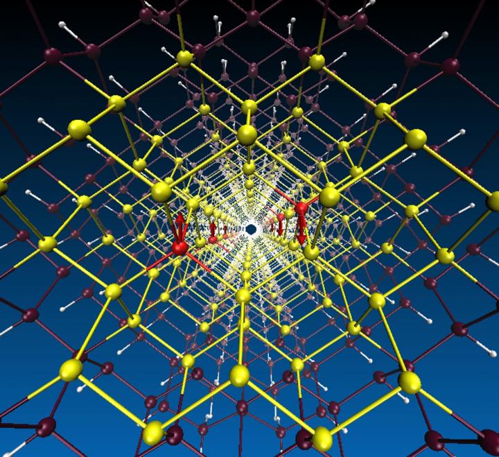
On their own antiferromagnetic materials aren’t great for electronic devices, but they’re not influenced by outside magnetic fields. This ability to resist magnetic manipulation started getting more attention from the research community and Pati’s team used a predictive quantum many-body theory that considers electron-electron interactions. The team found that chromium-doped nanowires with a germanium core and silicon shell can be an antiferromagnetic semiconductor.
Several research groups have recently demonstrated manipulation of individual magnetic states in antiferromagnetic materials using electrical current and lasers. They observed spin dynamics in the terahertz frequency — much faster than the frequency used in our current data storage devices. This observation has opened up a plethora of research interests in antiferromagnetism and could lead to faster, higher-capacity data storage.
“In our recent work, we have successfully harnessed the intriguing features of an antiferromagnet into a low-dimensional, complementary metal-oxide compatible semiconductor (CMOS) nanowire without destroying the semiconducting property of the nanowire,” Pati said. “This opens up possibilities for smaller and smarter electronics with higher capacity data storage and manipulation.”
Pati adds that the most exciting part of the research for his team was uncovering the mechanism that dictates antiferromagnetism. The mechanism is called superexchange and it controls the spin of electrons and the antiparallel alignment that makes them antiferromagnetic. In the team’s nanowire, germanium electrons act as a go-between, an exchanger, between unconnected chromium atoms.
“The interaction between the magnetic states of the chromium atoms is mediated by the intermediate atoms they are bonded to. It is a cooperative magnetic phenomenon,” Pati said. “In a simple way, let us say there are two people A and B: They are far apart and cannot communicate directly. But A has a friend C and B has a friend D. C and D are close friends. So, A and B can interact indirectly through C and D.”
Better understanding how electrons communicate between atomic friends enables more experiments to test the potential of materials like chromium-doped nanowires. Better understanding the germanium-silicon nanowire material’s antiferromagnetic nature is what boosts potential for smaller, smarter, higher capacity electronics.
###
Media Contact
Allison Mills
[email protected]
Original Source
https:/
Related Journal Article
http://dx.


