• HOME
  • NEWS
  • EXPLORE
    • CAREER
      • Companies
      • Jobs
    • EVENTS
    • iGEM
      • News
      • Team
    • PHOTOS
    • VIDEO
    • WIKI
  • BLOG
  • COMMUNITY
    • FACEBOOK
    • INSTAGRAM
    • TWITTER
Sunday, August 3, 2025
BIOENGINEER.ORG
No Result
View All Result
  • Login
  • HOME
  • NEWS
  • EXPLORE
    • CAREER
      • Companies
      • Jobs
        • Lecturer
        • PhD Studentship
        • Postdoc
        • Research Assistant
    • EVENTS
    • iGEM
      • News
      • Team
    • PHOTOS
    • VIDEO
    • WIKI
  • BLOG
  • COMMUNITY
    • FACEBOOK
    • INSTAGRAM
    • TWITTER
No Result
View All Result
Bioengineer.org
No Result
View All Result
Home NEWS Science News Science

Cambridge spin-out starts producing graphene at commercial scale

Bioengineer by Bioengineer
March 12, 2019
in Science
Reading Time: 2 mins read
0
Share on FacebookShare on TwitterShare on LinkedinShare on RedditShare on Telegram

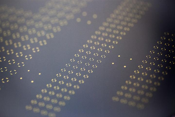
IMAGE

Credit: Paragraf

A recent University of Cambridge spin-out company, Paragraf, has started producing graphene – a sheet of carbon just one atomic layer thick – at up to eight inches in diameter, large enough for commercial electronic devices.

Paragraf is producing graphene ‘wafers’ and graphene-based electronic devices, which could be used in transistors, where graphene-based chips could deliver speeds more than ten times faster than silicon chips; and in chemical and electrical sensors, where graphene could increase sensitivity by a factor of more than 30. The company’s first device will be available in the next few months.

Graphene’s remarkable properties – stronger than steel, more conductive than copper, highly flexible and transparent – make it ideal for a range of applications. However, its widespread commercial application in electronic devices has been held back by the difficulties associated with producing it at high quality and at high volume. The conventional way of making large-area graphene involves using copper as a catalyst which contaminates the graphene, making it unsuitable for electronic applications.

Professor Sir Colin Humphreys from the Centre for Gallium Nitride in Cambridge’s Department of Materials Science and Metallurgy, along with his former postdoctoral researchers Dr Simon Thomas and Dr Ivor Guiney, developed a new way to make large-area graphene in 2015.

Using their method, the researchers were able form high-quality graphene wafers up to eight inches in diameter, beating not only other university research groups worldwide, but also companies like IBM, Intel and Samsung.

The three researchers spun out Paragraf in early 2018. Thomas is currently the company’s CEO and Guiney is its Chief Technology Officer, while Humphreys, who has recently moved to Queen Mary University of London, serves as Chair.

Paragraf has received £2.9 million in funding to support the development of its first commercial products and moved into premises in February 2018. The funding round was led by Cambridge Enterprise, the University’s commercialisation arm. Paragraf already employs 16 people and has filed eight patents.

“Paragraf has the potential to transform a wide range of industries, including electronics, energy and healthcare,” said Humphreys. “It will enable the brilliant basic science results achieved in laboratories worldwide using small graphene flakes to be commercially exploited in graphene-based devices and to realise the potential and benefits to society of graphene, the wonder material.”

###

The original research was funded by the Engineering and Physical Sciences Research Council (EPSRC).

Media Contact
Sarah Collins
[email protected]

Original Source

https://www.cam.ac.uk/research/news/cambridge-spin-out-starts-producing-graphene-at-commercial-scale

Tags: Electrical Engineering/ElectronicsMaterialsTechnology TransferTechnology/Engineering/Computer Science
Share13Tweet8Share2ShareShareShare2

Related Posts

Five or more hours of smartphone usage per day may increase obesity

July 25, 2019
IMAGE

NASA’s terra satellite finds tropical storm 07W’s strength on the side

July 25, 2019

NASA finds one burst of energy in weakening Depression Dalila

July 25, 2019

Researcher’s innovative flood mapping helps water and emergency management officials

July 25, 2019
Please login to join discussion

POPULAR NEWS

  • Blind to the Burn

    Overlooked Dangers: Debunking Common Myths About Skin Cancer Risk in the U.S.

    60 shares
    Share 24 Tweet 15
  • Neuropsychiatric Risks Linked to COVID-19 Revealed

    52 shares
    Share 21 Tweet 13
  • Dr. Miriam Merad Honored with French Knighthood for Groundbreaking Contributions to Science and Medicine

    46 shares
    Share 18 Tweet 12
  • Study Reveals Beta-HPV Directly Causes Skin Cancer in Immunocompromised Individuals

    38 shares
    Share 15 Tweet 10

About

We bring you the latest biotechnology news from best research centers and universities around the world. Check our website.

Follow us

Recent News

Detecting High Liver Tumor Burden in NETs

Expanded Subventricular Zone Aids Postnatal Interneuron Migration

Bipolar-Barrier Tunnels Boost Mid-Wave Infrared Detection

  • Contact Us

Bioengineer.org © Copyright 2023 All Rights Reserved.

Welcome Back!

Login to your account below

Forgotten Password?

Retrieve your password

Please enter your username or email address to reset your password.

Log In
No Result
View All Result
  • Homepages
    • Home Page 1
    • Home Page 2
  • News
  • National
  • Business
  • Health
  • Lifestyle
  • Science

Bioengineer.org © Copyright 2023 All Rights Reserved.