Credit: Source: UW Physics, A. Bogucki, W. Pacuski
For the first time, monolayers of transition metal dichalcogenides with excellent optical properties were grown. A team of physicists from the University of Warsaw managed to overcome the technical difficulties faced by industry and scientists from around the world, namely the very limited size, heterogeneity, and broadening of the spectral lines of fabricated materials. Monolayers without these defects were grown by molecular beam epitaxy on atomically flat boron nitride substrates.
Two-dimensional crystals with a honeycomb structure, including the famous graphene, have already revolutionized nanoscience and have the potential to revolutionize common technologies, as well. Therefore, it is highly desirable to develop industrial-scale methods for their production.
However, despite substantial investments in the development of growth techniques for atomically thin crystals, the best quality monolayers are currently still obtained using exfoliation, i.e. due to the mechanical detachment of individual atomic layers from the bulk crystal. For example, graphene flakes exfoliated from bulk graphite exhibit superior electrical properties when compared to grown graphene. In contrast, the size of the mechanically exfoliated monolayers is rather small.
Similarly, optical properties of two-dimensional transition metal dichalcogenides (e.g. molybdenum diselenide) are fully revealed only for layers obtained as a result of exfoliation and after having been subjected to further mechanical treatment, such as placing them between layers of boron nitride. However, as already mentioned, this technique does not lead to atomically thin crystals on a larger scale, resulting in heterogeneity, limited size, and even to the appearance of corrugations, bubbles, and irregular edges.
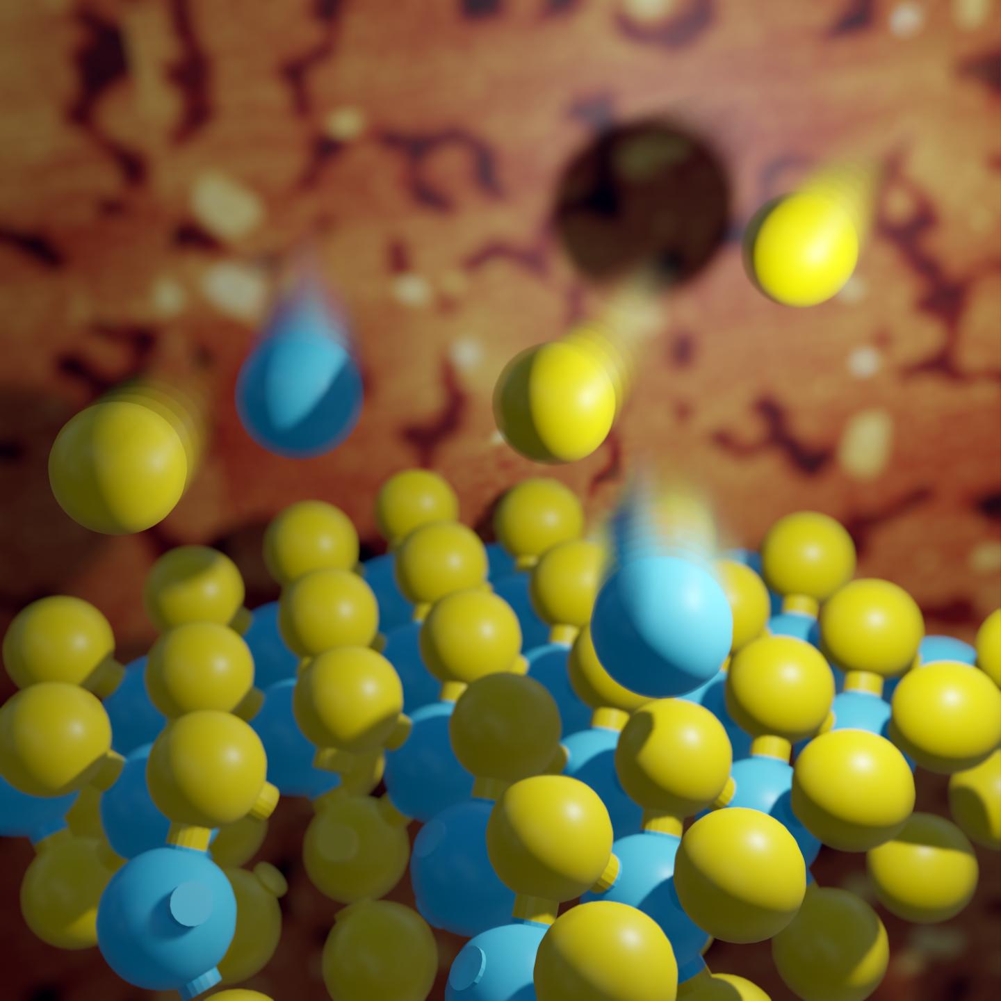
Hence, it is crucial to develop a technique for growing two-dimensional transition metal dichalcogenides that will allow for the production of monolayers with a large surface area. Currently, one of the most advanced technologies for producing thin semiconductor crystals is molecular beam epitaxy (MBE). It provides low-dimensional structures on large wafers, with high homogeneity, but its effectiveness in the production of transition metal dichalcogenides has been very limited so far. In particular, the optical properties of MBE grown monolayers have hitherto been rather modest, e.g. spectral lines have been broad and weak, giving no hope for the use of the spectacular optical properties of transition metal dichalcogenides on a larger scale.
It is in this area that researchers from the Faculty of Physics of the University of Warsaw made a breakthrough. In collaboration with several laboratories from Europe and Japan, they conducted a series of studies on the growth of transition metal dichalcogenides monolayers on an atomically flat boron nitride substrate. In this way, using the MBE method, they obtained flat crystals, equal in size to the substrate, showing uniform parameters over the entire surface, including – most valuably – excellent optical properties.
The results of the work have just been published in the latest volume of the prestigious journal Nano Letters. The discovery directs future research into the industrial production of atomically thin materials. In particular, it indicates the need to develop larger atomically flat boron nitride wafers. On such wafers, it will be possible to grow monolayers with the optical quality, dimensions, and homogeneity required for optoelectronic applications.
Physics and Astronomy first appeared at the University of Warsaw in 1816, under the then Faculty of Philosophy. In 1825 the Astronomical Observatory was established. Currently, the Faculty of Physics’ Institutes include Experimental Physics, Theoretical Physics, Geophysics, Department of Mathematical Methods and an Astronomical Observatory. Research covers almost all areas of modern physics, on scales from the quantum to the cosmological. The Faculty’s research and teaching staff includes ca. 200 university teachers, of which 87 are employees with the title of professor. The Faculty of Physics, University of Warsaw, is attended by ca. 1000 students and more than 170 doctoral students.
###
SCIENTIFIC PAPERS:
W. Pacuski, M. Grzeszczyk, K. Nogajewski, A. Bogucki, K. Oreszczuk, J. Kucharek, K.E. Polczynska, B. Seredynski, A. Rodek, R. Bozek, T. Taniguchi, K. Watanabe, S. Kret, J. Sadowski, T. Kazimierczuk, M. Potemski, P. Kossacki, ”Narrow Excitonic Lines and Large-Scale Homogeneity of Transition-Metal Dichalcogenide Monolayers Grown by Molecular Beam Epitaxy on Hexagonal Boron Nitride”, Nano Lett. 20, 3058 (2020).
DOI: https:/
CONTACTS:
Dr. hab. Wojciech Pacuski
Faculty of Physics, University of Warsaw
email: [email protected]
RELATED LINKS:
https:/
Laboratory of molecular beam epitaxy (MBE) web page
http://lumnp.
Laboratory of Ultrafast Magneto Spectroscopy (LUMS) web page
https:/
The Faculty of Physics, University of Warsaw web page
https:/
Press office of the Faculty of Physics, University of Warsaw
Media Contact
Wojciech Pacuski
[email protected]
Related Journal Article
http://dx.


