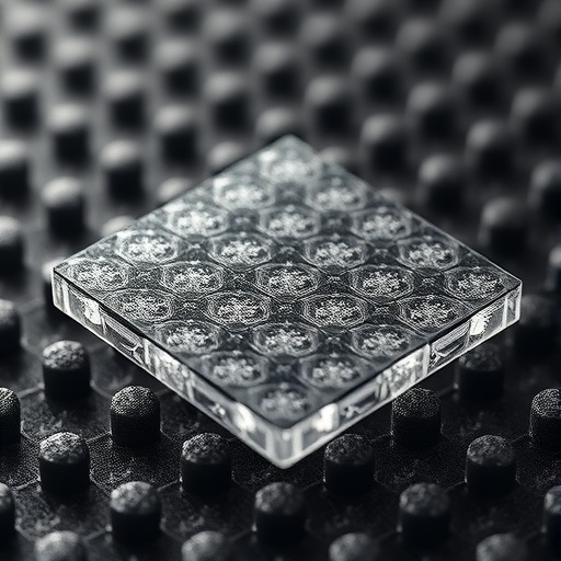
A material that is only a few atoms thick has emerged as a potential solution to one of modern electronics’ most stubborn problems: unwanted electrical interaction between neighboring components. In a study published in Nature Electronics, Chia T. Toh, Alexander K. Grebenko, U. Karadeniz and colleagues report atomically thin amorphous carbon with an unusually low dielectric constant. The finding could influence the design of future computer chips, sensors and nanoscale electronic systems, where controlling electric fields is becoming as important as carrying electrical current. Unlike conventional crystalline two-dimensional materials, the carbon described in the study lacks long-range atomic order, yet it retains a structure thin and uniform enough to function as an insulating layer.
The importance of the result lies in the role played by dielectric materials inside every integrated circuit. Conductive wires must be separated from one another, and those wires are usually surrounded by insulating films that prevent current from leaking between them. However, an insulator does not simply block electricity. It also responds to an electric field by becoming polarized, a process that allows it to store electrical energy. This behavior is quantified by the dielectric constant, which compares a material’s ability to become polarized with that of empty space. A lower dielectric constant means that the material stores less electrostatic energy and produces weaker capacitive coupling between adjacent conductors—an increasingly valuable property as electronic devices shrink.
Capacitance between neighboring interconnects can create a phenomenon known as crosstalk. When a voltage changes rapidly in one wire, the electric field surrounding it can influence a nearby wire, causing unwanted voltage fluctuations, timing errors and signal distortion. In high-performance processors, communication systems and densely packed memory circuits, these effects can limit speed and increase energy consumption. Engineers have responded by searching for “low-k” dielectrics, materials with reduced dielectric constants that can be placed between or around conductors. The challenge is to achieve a low electrical response without sacrificing mechanical strength, chemical stability, thermal performance or compatibility with semiconductor manufacturing.
The carbon film reported by the researchers is intriguing because it combines two characteristics that are rarely found together at the nanoscale. It is atomically thin, minimizing the physical distance that an insulating layer adds to a device, and it is amorphous, meaning that its atoms do not form the repeating lattice seen in graphite, diamond or many other crystalline solids. Amorphous materials can be easier to integrate over irregular surfaces because they do not depend on a particular crystal orientation. They may also avoid certain defects associated with grain boundaries, where separate crystalline domains meet. For advanced electronics, a material that can coat surfaces continuously while maintaining a very small dielectric response could offer a new route to reducing parasitic capacitance.
At the atomic level, the behavior of an insulator depends on how its electrons and atomic bonds respond when an electric field is applied. In a conventional dielectric, electrons shift slightly relative to atomic nuclei, while the atomic framework may also distort. These microscopic responses add together to produce the material’s macroscopic dielectric constant. In an ultrathin carbon network, the arrangement of bonds, the density of the film and the interfaces surrounding it can all influence this response. The amorphous structure described in the study therefore matters not merely as a structural curiosity: it may help determine how polarization is distributed through the film and how strongly the carbon interacts electrically with neighboring materials.
The reported advance also addresses a central limitation of many two-dimensional materials. Graphene, for example, is exceptionally thin and electrically remarkable, but its high conductivity prevents it from serving as a conventional insulating layer. Other atomically thin materials can act as dielectrics, yet their properties may vary with thickness, crystal orientation, defects or environmental exposure. An amorphous carbon dielectric could provide a more uniform alternative, particularly if it can be formed across large areas and deposited onto surfaces used in standard device fabrication. The study’s significance is consequently not limited to the numerical value of its dielectric constant; it is also about whether a nanoscale carbon film can deliver predictable insulation in a form compatible with real circuitry.
A low dielectric constant is not automatically enough to make a material useful in a chip. Engineers must also examine leakage current, breakdown strength, adhesion, roughness, thermal stability and resistance to chemical processing. An insulating layer must withstand the electric fields generated during operation without suddenly becoming conductive, and it must remain intact during the heating and etching steps used to manufacture devices. At atomic thicknesses, interfaces become especially important because a large fraction of the material is close to another substance. Charges trapped at those boundaries can alter the apparent dielectric behavior, while pinholes or local thinning can create pathways for electrical failure. The researchers’ work places this carbon material in that broader engineering context, where electrical performance must be balanced against reliability.
The potential applications extend beyond conventional processors. As transistors and interconnects approach atomic dimensions, ultrathin dielectrics could help separate control electrodes, isolate nanoscale wiring and reduce the energy lost to charging and discharging. Flexible electronics and three-dimensional chip architectures could also benefit from coatings capable of covering complex geometries without requiring thick insulating layers. In sensors, a small dielectric response may improve the ability to detect changes in nearby charges or molecules by reducing background capacitance. Photonic and quantum devices, which can be sensitive to fluctuating electric fields and material defects, may likewise gain from carefully engineered low-k interfaces. These possibilities remain prospective, but the combination of carbon chemistry and atomic-scale thickness makes the material unusually appealing.
The study arrives at a moment when the semiconductor industry is confronting the physical limits of miniaturization. For decades, shrinking transistors delivered faster and more efficient electronics, but modern systems are increasingly constrained by the wires connecting those transistors. Even when a transistor itself switches efficiently, the surrounding interconnect network can consume substantial energy as signals travel and capacitances are repeatedly charged. Reducing dielectric coupling is therefore a way to improve the entire system rather than a single component. Atomically thin amorphous carbon could become part of that strategy if further research confirms that its low dielectric response is reproducible, stable under operating conditions and scalable beyond laboratory demonstrations.
The result does not mean that a new generation of carbon-based chips is ready to replace existing technologies. Manufacturing scale, uniformity, defect control and long-term reliability will determine whether the material can move from an advanced materials study into commercial devices. Researchers will also need to establish how the film behaves when integrated with metals, semiconductors and other insulating layers, and whether its properties remain unchanged during repeated heating, electrical cycling and exposure to fabrication chemicals. Even so, the work offers a striking example of how changing the atomic organization of a familiar element can produce a technologically valuable material. Carbon, already the foundation of graphene, diamond and countless molecular structures, may now provide an ultrathin shield against the unwanted electric fields that threaten the next era of electronics.
Subject of Research: Atomically thin amorphous carbon as an ultralow-dielectric-constant insulating material for nanoscale electronics.
Article Title: Atomically thin amorphous carbon with an ultralow dielectric constant
Article References: Toh, CT., Grebenko, A.K., Karadeniz, U. et al. “Atomically thin amorphous carbon with an ultralow dielectric constant.” Nature Electronics (2026). https://doi.org/10.1038/s41928-026-01685-2
Image Credits: AI Generated
DOI: https://doi.org/10.1038/s41928-026-01685-2
Keywords: amorphous carbon, ultralow dielectric constant, two-dimensional materials, low-k dielectrics, semiconductor technology, nanoscale electronics, crosstalk, interconnects
Tags: advanced dielectric materials for next-generation devicesatomically thin amorphous carbonatomically thin insulating layerselectrical field control in nanosystemsimpact of amorphous carbon on chip designlow dielectric constant for integrated circuitsnanoscale electronic insulationnon-crystalline 2D materials for electronicspolarized dielectric materials in electronicstwo-dimensional amorphous carbonultralow dielectric constant materialsultrathin dielectric films for sensors