Silicon-based electronics are approaching their physical limitations and new materials are needed to keep up with current technological demands. Two-dimensional (2D) materials have a rich array of properties, including superconductivity and magnetism, and are promising candidates for use in electronic systems, such as transistors. However, precisely controlling the properties of these materials is extraordinarily difficult.
Credit: The Grainger College of Engineering at University of Illinois Urbana-Champaign
Silicon-based electronics are approaching their physical limitations and new materials are needed to keep up with current technological demands. Two-dimensional (2D) materials have a rich array of properties, including superconductivity and magnetism, and are promising candidates for use in electronic systems, such as transistors. However, precisely controlling the properties of these materials is extraordinarily difficult.
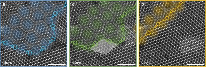
In an effort to understand how and why 2D interfaces take on the structures they do, researchers at the University of Illinois Urbana-Champaign have developed a method to visualize the thermally-induced rearrangement of 2D materials, atom-by-atom, from twisted to aligned structures using transmission electron microscopy (TEM). They observed a new and unexpected mechanism for this process where a new grain was seeded within one monolayer, whose structure was templated by the adjacent layer. Being able to control the macroscopic twist between layers allows for more control over the properties of the entire system.
This research, led by materials science & engineering professor Pinshane Huang and postdoctoral researcher Yichao Zhang, was recently published in the journal Science Advances.
“How the interfaces of the bilayer align with each other and through what mechanism they transform into a different configuration is very important,” Zhang says. “It controls the properties of the entire bilayer system which, in turn, affects both its nanoscale and microscopic behavior.”
The structure and properties of 2D multilayers are often highly heterogeneous and vary widely between samples and even within an individual sample. Two devices with just a few degrees of twist between layers could have different behavior. 2D materials are also known to reconfigure under external stimuli such as heating, which occurs during the fabrication process of electronic devices.
“People usually think of the two layers like having two sheets of paper twisted 45° to each other. To get the layers to go from twisted to aligned, you would just rotate the entire piece of paper,” Zhang says. “But what we found, actually, is it has a nucleus—a localized nanoscale aligned domain—and this domain grows larger and larger in size. Given the correct conditions, this aligned domain could take over the entire size of the bilayer.”
While researchers have speculated that this may happen, there hasn’t been any direct visualization at the atomic scale proving or disproving the theory. Zhang and the other researchers, however, were able to directly track the movement of individual atoms to see the tiny, aligned domain grow. They also observed that aligned regions could form at relatively low temperatures, ~200°C, in the range of typical processing temperatures for 2D devices.
There aren’t cameras small enough and fast enough to capture atomic dynamics. How then was the team able to visualize this atom-by-atom movement? The solution is very unique. They first encapsulated the twisted bilayer in graphene, essentially building a little reaction chamber around it, to look at the bilayer at atomic resolution as it was heated. Encapsulation by graphene helps to hold the atoms of the bilayer in place so that any structural transformation could be observed rather than the lattice getting destroyed by high-energy electrons of the TEM.
The encapsulated bilayer was then put on a chip that could be heated and cooled quickly. To capture the fast atomic dynamics, the sample underwent half second heat pulses between 100-1000°C. After each pulse, the team would look at where the atoms were using TEM and then repeated the process. “You can actually watch the system as it changes, as the atoms settle in from whatever configuration they were put in initially, to the configuration that is energetically favorable, that they want to be in,” Huang explains. “That can help us understand both the initial structure as it is fabricated and how it evolves with heat.”
Understanding how rearrangement happens can help tune the interfacial alignment at the nanoscale. “It is impossible to underscore how excited people are about that tuneability,” Huang says. “The macroscopic twist between the two layers is a really important parameter because as you rotate one on the other, you can actually change the properties of the entire system. For example, if you rotate the 2D material graphene to a specific angle, it becomes superconducting. For some materials, if you rotate them, you change the bandgap which changes the color of light it absorbs and what energy of light it emits. All of those things you change by altering the orientation of atoms between layers.”
*
Pinshane Huang is also the associate director of the Materials Research Laboratory at UIUC.
Other contributors to this work include Ji-Hwan Baek (co-first author, department of materials science and engineering, Seoul National University, Korea), Chia-Hao Lee (department of materials science and engineering, UIUC), Yeonjoon Jung (department of materials science and engineering, Seoul National University, Korea), Seong Chul Hong (department of materials science and engineering, Seoul National University, Korea), Gillian Nolan (department of materials science and engineering, UIUC), Kenji Watanabe (Research Center for Electronic and Optical Materials, National Institute for Materials Science, Japan), Takashi Taniguchi (Research Center for Materials Nanoarchitectonics, National Institute for Materials Science, Japan) and Gwan-Hyoung Lee (department of materials science and engineering, Seoul National University, Korea).
This research was funded by the U.S. Department of Energy, the Japan Society for the Promotion of Science and the Korean National Research Foundation.
DOI: 10.1126/sciadv.adk1874
https://www.science.org/doi/10.1126/sciadv.adk1874
Journal
Science Advances
DOI
10.1126/sciadv.adk1874
Article Publication Date
27-Mar-2024


