Credit: Sangheon Oh/Nature Nanotechnology
Training neural networks to perform tasks, such as recognizing images or navigating self-driving cars, could one day require less computing power and hardware thanks to a new artificial neuron device developed by researchers at the University of California San Diego. The device can run neural network computations using 100 to 1000 times less energy and area than existing CMOS-based hardware.
Researchers report their work in a paper published Mar. 18 in Nature Nanotechnology.
Neural networks are a series of connected layers of artificial neurons, where the output of one layer provides the input to the next. Generating that input is done by applying a mathematical calculation called a non-linear activation function. This is a critical part of running a neural network. But applying this function requires a lot of computing power and circuitry because it involves transferring data back and forth between two separate units–the memory and an external processor.
Now, UC San Diego researchers have developed a nanometer-sized device that can efficiently carry out the activation function.
“Neural network computations in hardware get increasingly inefficient as the neural network models get larger and more complex,” said Duygu Kuzum, a professor of electrical and computer engineering at the UC San Diego Jacobs School of Engineering. “We developed a single nanoscale artificial neuron device that implements these computations in hardware in a very area- and energy-efficient way.”
The new study, led by Kuzum and her Ph.D. student Sangheon Oh, was performed in collaboration with a DOE Energy Frontier Research Center led by UC San Diego physics professor Ivan Schuller, which focuses on developing hardware implementations of energy-efficient artificial neural networks.
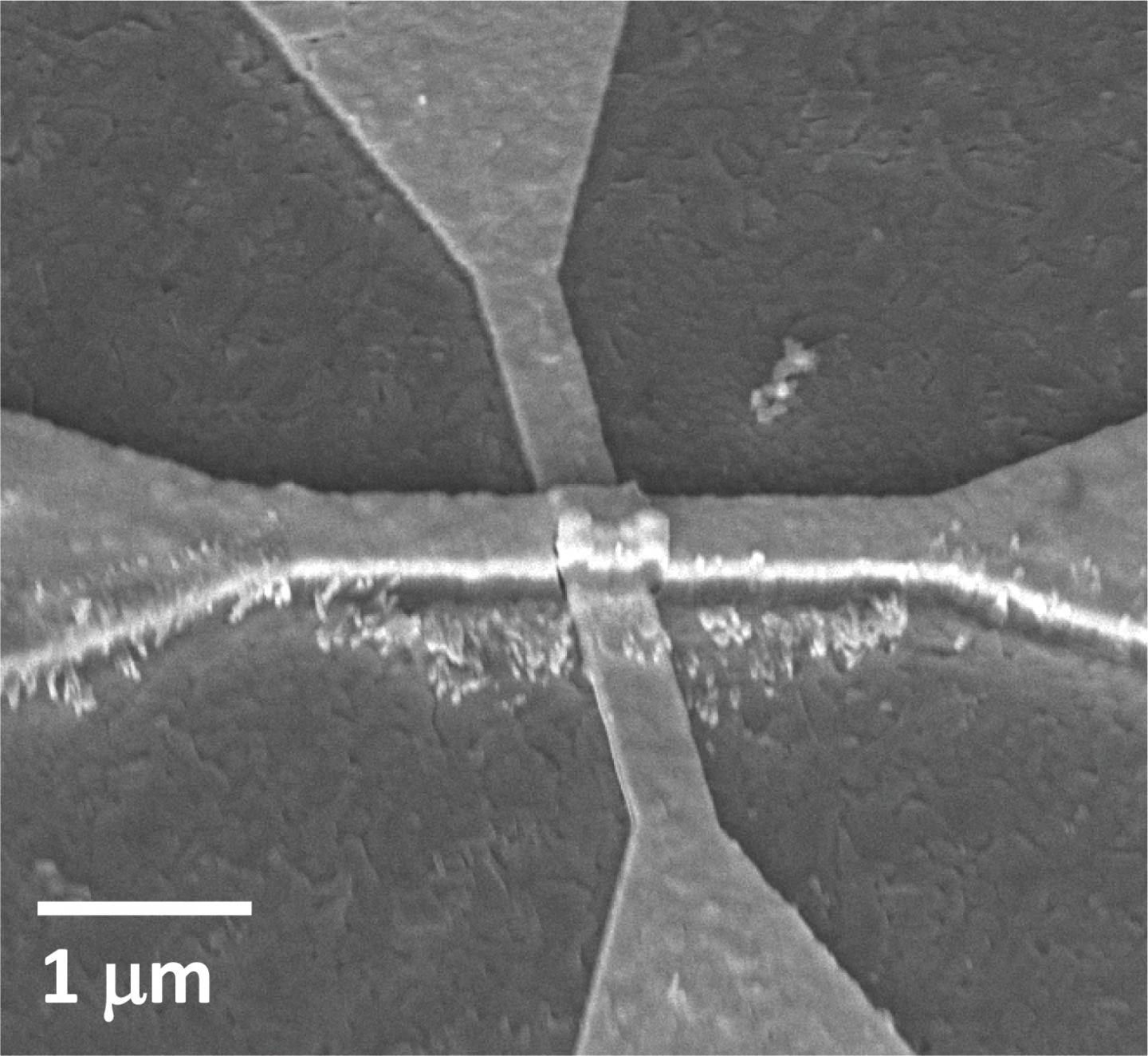
The device implements one of the most commonly used activation functions in neural network training called a rectified linear unit. What’s particular about this function is that it needs hardware that can undergo a gradual change in resistance in order to work. And that’s exactly what the UC San Diego researchers engineered their device to do–it can gradually switch from an insulating to a conducting state, and it does so with the help of a little bit of heat.
This switch is what’s called a Mott transition. It takes place in a nanometers-thin layer of vanadium dioxide. Above this layer is a nanowire heater made of titanium and gold. When current flows through the nanowire, the vanadium dioxide layer slowly heats up, causing a slow, controlled switch from insulating to conducting.
“This device architecture is very interesting and innovative,” said Oh, who is the study’s first author. Typically, materials in a Mott transition experience an abrupt switch from insulating to conducting because the current flows directly through the material, he explained. “In this case, we flow current through a nanowire on top of the material to heat it and induce a very gradual resistance change.”
To implement the device, the researchers first fabricated an array of these so-called activation (or neuron) devices, along with a synaptic device array. Then they integrated the two arrays on a custom printed circuit board and connected them together to create a hardware version of a neural network.
The researchers used the network to process an image–in this case, a picture of Geisel Library at UC San Diego. The network performed a type of image processing called edge detection, which identifies the outlines or edges of objects in an image. This experiment demonstrated that the integrated hardware system can perform convolution operations that are essential for many types of deep neural networks.
The researchers say the technology could be further scaled up to do more complex tasks such as facial and object recognition in self-driving cars. With interest and collaboration from industry, this could happen, noted Kuzum.
“Right now, this is a proof of concept,” Kuzum said. “It’s a tiny system in which we only stacked one synapse layer with one activation layer. By stacking more of these together, you could make a more complex system for different applications.”
###
Paper: “Energy Efficient Mott Activation Neuron for Full Hardware Implementation of Neural Networks.”
This work was supported by the Office of Naval Research, Samsung Electronics, the National Science Foundation, the National Institutes of Health, a Qualcomm Fellowship and the U.S. Department of Energy, Office of Science through an Energy Frontier Research Center.
Media Contact
Liezel Labios
[email protected]
Related Journal Article
http://dx.

