• HOME
  • NEWS
  • EXPLORE
    • CAREER
      • Companies
      • Jobs
    • EVENTS
    • iGEM
      • News
      • Team
    • PHOTOS
    • VIDEO
    • WIKI
  • BLOG
  • COMMUNITY
    • FACEBOOK
    • INSTAGRAM
    • TWITTER
Thursday, April 9, 2026
BIOENGINEER.ORG
No Result
View All Result
  • Login
  • HOME
  • NEWS
  • EXPLORE
    • CAREER
      • Companies
      • Jobs
        • Lecturer
        • PhD Studentship
        • Postdoc
        • Research Assistant
    • EVENTS
    • iGEM
      • News
      • Team
    • PHOTOS
    • VIDEO
    • WIKI
  • BLOG
  • COMMUNITY
    • FACEBOOK
    • INSTAGRAM
    • TWITTER
No Result
View All Result
Bioengineer.org
No Result
View All Result
Home NEWS Science News Chemistry

An ultimate one-dimensional electronic channel in hexagonal boron nitride

Bioengineer by Bioengineer
March 9, 2020
in Chemistry
Reading Time: 3 mins read
0
IMAGE
Share on FacebookShare on TwitterShare on LinkedinShare on RedditShare on Telegram

A zero bandgap boundary discovered in insulating hexagonal boron nitride sheets with could pave the way for new nano-electronic devices

IMAGE

Credit: IBS


In the field of 2D electronics, the norm used to be that graphene is the main protagonist and hexagonal boron nitride (hBN) is its insulating passive support. Researchers of the Center for Multidimensional Carbon Materials (CMCM) within the Institute for Basic Science (IBS, South Korea) made a discovery that might change the role of hBN. They have reported that stacking of ultrathin sheets of hBN in a particular way creates a conducting boundary with zero bandgap. In other words, the same material could block the flow of electrons, as a good insulator, and also conduct electricity in a specific location. Published in the journal Science Advances, this result is expected to raise interest in hBN by giving it a more active part in 2D electronics.

Similarly to graphene, hBN is a 2D material with high chemical, mechanical and thermal stability. hBN sheets resemble a chicken wire, and are made of hexagonal rings of alternating boron and nitrogen atoms, strongly bound together. However, unlike graphene, hBN is an insulator with a large bandgap of more than five electronVolts, which limits its applications.

“In contrast to the wide spectrum of proposed applications for graphene, hexagonal boron nitride is often regarded as an inert material, largely confined as substrate or electron barrier for 2D material-based devices. When we began this research, we were convinced that reducing the bandgap of hBN could give to this material the versatility of graphene,” says the first author, Hyo Ju Park.

Several attempts to lower the bandgap of hBN have been mostly ineffective because of its strong covalent boron-nitrogen bonds and chemical inertness. IBS researchers in collaboration with colleagues of Ulsan National Institute of Science and Technology (UNIST), Sejong University, Korea, and Nanyang Technological University, Singapore, managed to produce a particular stacking boundary of a few hBN layers having a bandgap of zero electronVolts.

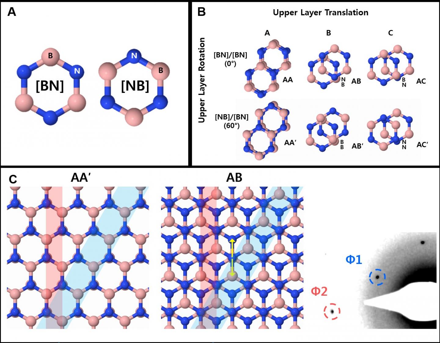
Depending on how the hBN sheets are piled up, the material can assume different configurations. For example, in the so-called AA? arrangement, the atoms in one layer are aligned directly on the top of atoms in another layer, but successive layers are rotated such that boron is located on nitrogen and nitrogen on boron atoms. In another type of layout, known as AB, half of the atoms of one layer lie directly over the center of the hexagonal rings of the lower sheet, and the other atoms overlap with the atoms underneath.

For the first time, the team has reported atomically sharp AA?/AB stacking boundaries formed in few-layer hBN grown by chemical vapor deposition. Characterized by a line of oblong hexagonal rings, this specific boundary has zero bandgap. To confirm this result, the research performed several simulations and tests via transmission electron microscopy, density functional theory calculations, and ab initio molecular dynamics simulations.

“An atomic conducting channel expands the application range of boron nitride infinitely, and opens new possibilities for all-hBN or all 2D nanoelectronic devices,” points out the corresponding author Zonghoon Lee.

###

Media Contact
Zonghoon Lee
[email protected]

Related Journal Article

http://dx.doi.org/10.1126/sciadv.aay4958

Tags: Chemistry/Physics/Materials Sciences
Share12Tweet8Share2ShareShareShare2

Related Posts

Insilico Achieves Breakthrough in Cancer Therapy by Uncovering Selective PKMYT1 Inhibitors Through Sulfur-Lone Pair Interactions

Insilico Achieves Breakthrough in Cancer Therapy by Uncovering Selective PKMYT1 Inhibitors Through Sulfur-Lone Pair Interactions

April 9, 2026
Unveiling Graphene’s Role in Photocatalytic Composites Through Theoretical Modeling

Unveiling Graphene’s Role in Photocatalytic Composites Through Theoretical Modeling

April 9, 2026

Nanocomposite Hydrogel Patch Enables Sequential Treatment for Postoperative Tumor Eradication, Immune Modulation, and Tissue Regeneration Following Melanoma Surgery

April 9, 2026

Breakthrough AI Technology Accelerates Drug Development Process

April 9, 2026
Please login to join discussion

POPULAR NEWS

  • blank

    Revolutionary AI Model Enhances Precision in Detecting Food Contamination

    98 shares
    Share 39 Tweet 25
  • Imagine a Social Media Feed That Challenges Your Views Instead of Reinforcing Them

    1012 shares
    Share 400 Tweet 250
  • Popular Anti-Aging Compound Linked to Damage in Corpus Callosum, Study Finds

    44 shares
    Share 18 Tweet 11
  • Revolutionary Theory Transforms Quantum Perspective on the Big Bang

    40 shares
    Share 16 Tweet 10

About

We bring you the latest biotechnology news from best research centers and universities around the world. Check our website.

Follow us

Recent News

Innovative 10K Liquid SNP Genotyping Array Developed for Wax Gourd

Risk of Colorectal Cancer and Mortality in Older Adults: Impact of Adenoma Detection on Previous Colonoscopy

Children with the greatest dental care needs are the least likely to benefit from school-based programs

Subscribe to Blog via Email

Enter your email address to subscribe to this blog and receive notifications of new posts by email.

Join 78 other subscribers
  • Contact Us

Bioengineer.org © Copyright 2023 All Rights Reserved.

Welcome Back!

Login to your account below

Forgotten Password?

Retrieve your password

Please enter your username or email address to reset your password.

Log In
No Result
View All Result
  • Homepages
    • Home Page 1
    • Home Page 2
  • News
  • National
  • Business
  • Health
  • Lifestyle
  • Science

Bioengineer.org © Copyright 2023 All Rights Reserved.