The precisely controlled photon source, made from an atomically thin semiconducting material, could aid the development of advanced quantum communication
Credit: Berkeley Lab
Secure telecommunications networks and rapid information processing make much of modern life possible. To provide more secure, faster, and higher-performance information sharing than is currently possible, scientists and engineers are designing next-generation devices that harness the rules of quantum physics. Those designs rely on single photons to encode and transmit information across quantum networks and between quantum chips. However, tools for generating single photons do not yet offer the precision and stability required for quantum information technology.
Now, as reported recently in the journal Science Advances, researchers have found a way to generate single, identical photons on demand. By positioning a metallic probe over a designated point in a common 2D semiconductor material, the team led by researchers at the U.S. Department of Energy’s Lawrence Berkeley National Laboratory (Berkeley Lab) has triggered a photon emission electrically. The photon’s properties may be simply adjusted by changing the applied voltage.
“The demonstration of electrically driven single-photon emission at a precise point constitutes a big step in the quest for integrable quantum technologies,” said Alex Weber-Bargioni, a staff scientist at Berkeley Lab’s Molecular Foundry who led the project. The research is part of the Center for Novel Pathways to Quantum Coherence in Materials (NPQC), an Energy Frontier Research Center sponsored by the Department of Energy, whose overarching goal is to find new approaches to protect and control quantum memory that can provide new insights into novel materials and designs for quantum computing technology.
Photons are one of the most robust carriers of quantum information and can travel long distances without losing their memory, or so-called coherence. To date, most established schemes for secure communication transfer that will power large-scale quantum communications require light sources to generate one photon at a time. Each photon must have a precisely defined wavelength and orientation. The new photon emitter demonstrated at Berkeley Lab achieves that control and precision. It could be used for transferring information between quantum processors on different chips, and ultimately scaled up to larger processors and a future quantum internet that links sophisticated computers around the world.
The photon emitter is based on a common 2D semiconductor material (tungsten disulfide, WS2), which has a sulfur atom removed from its crystal structure. That carefully located atomic imperfection, or defect, serves as a point where the photon can be generated through application of an electric current.
The challenge is not how to generate single photons, but how to make them truly identical and produce them on demand. Photon-emitting devices, like the semiconductor nanoparticles or “quantum dots” that light up QLED TVs, that are fabricated by lithography are subject to inherent variability, since no pattern-based system can be identical down to a single atom. Researchers working with Weber-Bargioni took a different approach by growing a thin-film material on a sheet of graphene. Any impurities introduced to the thin film’s atomic structure are repeated and identical throughout the sample. Through simulations and experiments, the team determined just where to introduce an imperfection to the otherwise uniform structure. Then, by applying an electrical contact to that location, they were able to trigger the material to emit a photon and control its energy with the applied voltage. That photon is then available to carry information to a distant location.
“Single-photon emitters are like a terminal where carefully prepared but fragile quantum information is sent on a journey into a lightning-fast, sturdy box,” said Bruno Schuler, a postdoctoral researcher at the Molecular Foundry (now a research scientist at Empa – the Swiss Federal Laboratories for Materials Science and Technology) and lead author of the work.
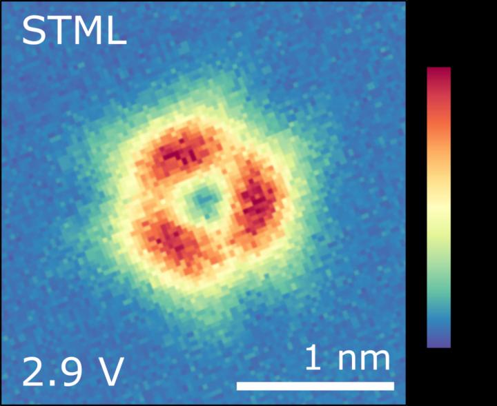
Key to the experiment is the gold-coated tip of a scanning tunnelling microscope that can be positioned exactly over the defect site in the thin film material. When a voltage is applied between the probe tip and the sample, the tip injects an electron into the defect. When the electron travels or tunnels from the probe tip, a well-defined part of its energy gets transformed into a single photon. Finally, the probe tip acts as an antenna that helps guide the emitted photon to an optical detector which records its wavelength and position.
By mapping the photons emitted from thin films made to include various defects, the researchers were able to pinpoint the correlation between the injected electron, local atomic structure, and the emitted photon. Usually, the optical resolution of such a map is limited to a few hundred nanometers. Thanks to extremely localized electron injection, combined with state-of-the-art microscopy tools, the Berkeley Lab team could determine where in the material a photon emerged with a resolution below 1 angstrom, about the diameter of a single atom. The detailed photon maps were crucial to pinpointing and understanding the electron-triggered photon emission mechanism.
“In terms of technique, this work has been a great breakthrough because we can map light emission from a single defect with sub-nanometer resolution. We visualize light emission with atomic resolution,” said Katherine Cochrane, a postdoctoral researcher at the Molecular Foundry and a lead author on the paper.
Defining single-photon light sources in two-dimensional materials with atomic precision provides unprecedented insight critical to understanding how those sources work, and provides a strategy for making groups of perfectly identical ones. The work is part of NPQC’s focus on exploring novel quantum phenomena in nonhomogenous 2D materials.
Two-dimensional materials are leading the way as a powerful platform for next-generation photon emitters. The thin films are flexible and easily integrated with other structures, and now provide a systematic way for introducing unparalleled control over photon emission. Based on the new results, the researchers plan to work on employing new materials to use as photon sources in quantum networks and quantum simulations.
###
This research was supported by the DOE Office of Science and grants from the Swiss National Science Foundation.
The Molecular Foundry is a DOE Office of Science user facility located at Berkeley Lab.
Founded in 1931 on the belief that the biggest scientific challenges are best addressed by teams, Lawrence Berkeley National Laboratory and its scientists have been recognized with 14 Nobel Prizes. Today, Berkeley Lab researchers develop sustainable energy and environmental solutions, create useful new materials, advance the frontiers of computing, and probe the mysteries of life, matter, and the universe. Scientists from around the world rely on the Lab’s facilities for their own discovery science. Berkeley Lab is a multiprogram national laboratory, managed by the University of California for the U.S. Department of Energy’s Office of Science.
DOE’s Office of Science is the single largest supporter of basic research in the physical sciences in the United States, and is working to address some of the most pressing challenges of our time. For more information, please visit energy.gov/science.
Media Contact
Laurel Kellner
[email protected]
Original Source
https:/
Related Journal Article
http://dx.


