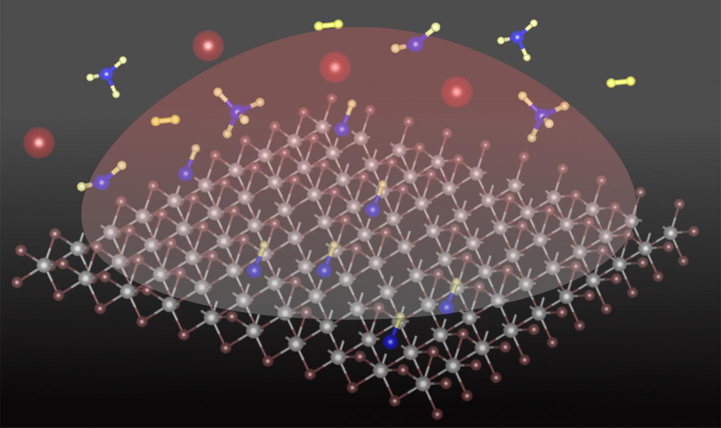
Credit: Fu Zhang/Penn State
A technique that introduces carbon-hydrogen molecules into a single atomic layer of the semiconducting material tungsten disulfide dramatically changes the electronic properties of the material, according to Penn State researchers at Penn State who say they can create new types of components for energy-efficient photoelectric devices and electronic circuits with this material.
“We have successfully introduced the carbon species into the monolayer of the semiconducting material,” said Fu Zhang, doctoral student in materials science and engineering lead author of a paper published online today (May26) in Science Advances.
Prior to doping – adding carbon – the semiconductor, a transition metal dichalcogenide (TMD), was n-type — electron conducting. After substituting carbon atoms for sulfur atoms, the one-atom-thick material developed a bipolar effect, a p-type — hole — branch, and an n-type branch. This resulted in an ambipolar semiconductor.
“The fact that you can change the properties dramatically by adding as little as two atomic percent was something unexpected,” Mauricio Terrones, senior author and distinguished professor of physics, chemistry and materials science and engineering.
According to Zhang, once the material is highly doped with carbon, the researchers can produce a degenerate p-type with a very high carrier mobility. “We can build n+/p/n+ and p+/n/p+ junctions with properties that have not been seen with this type of semiconductor,” he said.
In terms of applications, semiconductors are used in various devices in industry. In this case, most of those devices will be transistors of different sorts. There are around 100 trillion transistors in a laptop.
“This type of material might also be good for electrochemical catalysis,” Terrones said. “You could improve conductivity of the semiconductor and have catalytic activity at the same time.”
There are few papers in the field of 2D materials doping, because it requires multiple processes to take place simultaneously under specific types of conditions. The team’s technique uses a plasma to lower the temperature at which methane can be cracked – split apart – down to 752 degrees Fahrenheit. At the same time, the plasma has to be strong enough to knock a sulfur atom out of the atomic layer and substitute a carbon-hydrogen unit.
“It’s not easy to dope monolayers, and then to measure carrier transport is not trivial,” Terrones says. “There is a sweet spot where we are working. Many other things are required.”
Susan Sinnott, professor and head of the Department of Materials Science and Engineering, provided theoretical calculations that guided the experimental work. When Terrones and Zhang observed that doping the 2D material was changing its optical and electronic properties – something they had never seen before – Sinnott’s team predicted the best atom to dope with and predicted the properties, which corresponded with the experiment.
Saptarshi Das, assistant professor of engineering science and mechanics, and his group, then measured the carrier transport in various transistors with increasing amounts of carbon substitution. They watched the conductance change radically until they had completely changed the conduction type from negative to positive.
“It was very much a multidisciplinary work,” Terrones says.
###
Additional authors on the Science Advances paper, titled “Carbon doping of WS2 monolayers: Bandgap reduction and p-type doping transport,” include current or former doctoral students Yanfu Lu, Daniel Schulman, Tianyi Zhang, Zhong Lin and Yu Lei; and Ana Laura Ellias and Kazunori Fujisawa, assistant research professors of physics.
The Basic Energy Sciences program in the Department of Energy’s Office of Science supported this work.
Media Contact
A’ndrea Elyse Messer
[email protected]