
Credit: Christoph Hohmann / Nanosystems Initiative Munich
Modern computer technology is based on the transport of electric charge in semiconductors. But this technology's potential will be reaching its limits in the near future, since the components deployed cannot be miniaturized further. But, there is another option: using an electron's spin, instead of its charge, to transmit information. A team of scientists from Munich and Kyoto is now demonstrating how this works.
Computers and mobile devices continue providing ever more functionality. The basis for this surge in performance has been progressively extended miniaturization. However, there are fundamental limits to the degree of miniaturization possible, meaning that arbitrary size reductions will not be possible with semiconductor technology.
Researchers around the world are thus working on alternatives. A particularly promising approach involves so-called spin electronics. This takes advantage of the fact that electrons possess, in addition to charge, angular momentum – the spin. The experts hope to use this property to increase the information density and at the same time the functionality of future electronics.
Together with colleagues at the Kyoto University in Japan scientists at the Walther-Meißner-Institute (WMI) and the Technical University of Munich (TUM) in Garching have now demonstrated the transport of spin information at room temperature in a remarkable material system.
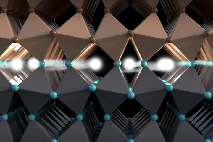
A unique boundary layer
In their experiment, they demonstrated the production, transport and detection of electronic spins in the boundary layer between the materials lanthanum-aluminate (LaAlO2) and strontium-titanate (SrTiO3). What makes this material system unique is that an extremely thin, electrically conducting layer forms at the interface between the two non-conducting materials: a so-called two-dimensional electron gas.
The German-Japanese team has now shown that this two-dimensional electron gas transports not only charge, but also spin. "To achieve this we first had to surmount several technical hurdles," says Dr Hans Hübl, scientist at the Chair for Technical Physics at TUM and Deputy Director of the Walther-Meißner-Institute. "The two key questions were: How can spin be transferred to the two-dimensional electron gas and how can the transport be proven?"
Information transport via spin
The scientists solved the problem of spin transfer using a magnetic contact. Microwave radiation forces its electrons into a precession movement, analogous to the wobbling motion of a top. Just as in a top, this motion does not last forever, but rather, weakens in time – in this case by imparting its spin onto the two-dimensional electron gas.
The electron gas then transports the spin information to a non-magnetic contact located one micrometer next to the contact. The non-magnetic contact detects the spin transport by absorbing the spin, building up an electric potential in the process. Measuring this potential allowed the researchers to systematically investigate the transport of spin and demonstrate the feasibility of bridging distances up to one hundred times larger than the distance of today's transistors.
Based on these results, the team of scientists is now researching to what extent spin electronic components with novel functionality can be implemented using this system of materials.
###
The research was funded by the German Research Foundation (DFG) in the context of the Cluster of Excellence "Nanosystems Initiative Munich" (NIM).
Publication:
Strong evidence for d-electron spin transport at room temperature at a LaAlO3/SrTiO3 interface. R. Ohshima, Y. Ando, K. Matsuzaki, T. Susaki, M. Weiler, S. Klingler, H. Huebl, E. Shikoh, T. Shinjo, S.T.B Goennenwein and M. Shiraishi. Nature Materials, Advanced Online Publication 13. Februar 2017.
Media Contact
Dr. Andreas Battenberg
[email protected]
49-892-891-0510
@TU_Muenchen
http://www.tum.de
############
Story Source: Materials provided by Scienmag


