


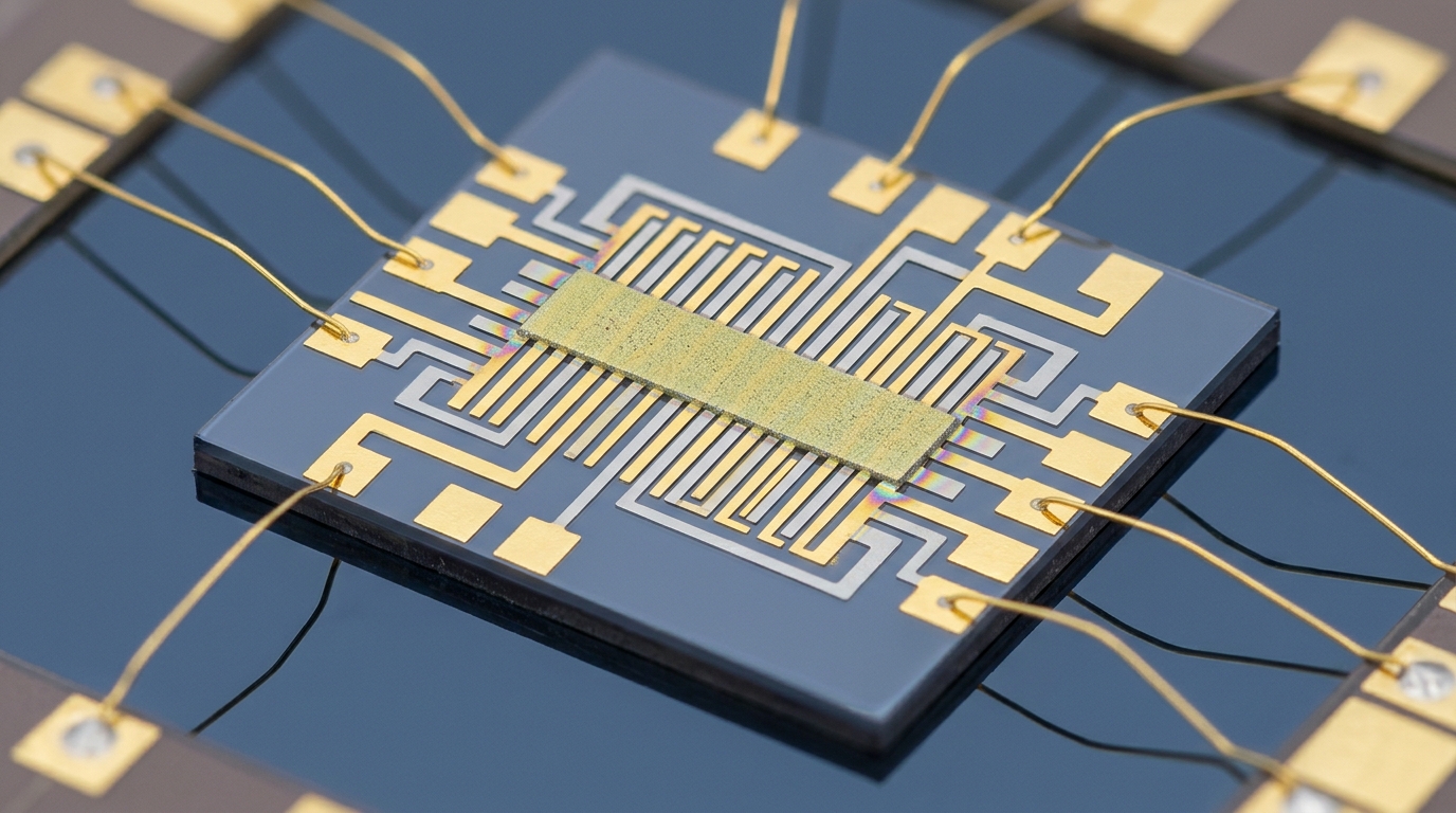
In bottom-gate tungsten trioxide devices engineered to detect nitrogen dioxide at room temperature, configurations exhibiting comparatively modest electrical metrics delivered substantially superior gas detection capabilities compared to higher-performing transistor designs.
Thin film transistors fabricated from metal oxides offer potential advantages for modern gas sensing architectures because they integrate detection capability directly with built-in signal amplification. A central question in the development of these devices has been whether optimizing baseline electrical parameters inevitably yields superior chemical detection. To address this uncertainty, investigators developed and compared two bottom-gate tungsten trioxide transistor configurations differing specifically in their source and drain contact metallization.
The experimental devices were prepared using radio frequency sputtering techniques to deposit the tungsten trioxide semiconductor layer. Material characterization confirmed that the deposited tungsten trioxide formed a monoclinic crystal structure exhibiting a preferred (002) crystallographic orientation, with an average crystallite size measured at 9.7 nanometers. The fabricated devices were designated according to their contact metals, with silver contacts incorporated into bottom-gate device BG TFT-1 and palladium contacts integrated into bottom-gate device BG TFT-2.
Comprehensive physical and electrical evaluations were conducted to examine the behavior of both transistor architectures. The characterization regimen included scanning electron microscopy, X-ray diffraction, output drain current versus drain voltage measurements, transfer drain current versus gate voltage sweeps, capacitance-frequency evaluations, and capacitance-gate voltage analyses. Key transistor parameters, including field-effect mobility, transconductance, threshold voltage, sub-threshold swing, and on-off current ratios, were measured to evaluate interface quality, dielectric behavior, gate modulation, and charge transport dynamics.
Both device configurations demonstrated stable transistor operation along with fully reversible sensing behavior when exposed to nitrogen dioxide gas concentrations ranging between 0.1 and 10 parts per million at ambient room temperature. Electrical testing showed that the palladium-contact device, BG TFT-2, achieved superior intrinsic electrical metrics, registering a field-effect mobility of 8.6 × 10⁻³ cm² V⁻¹ s⁻¹, alongside higher transconductance and a larger on-off current ratio than its silver-contact counterpart.
Despite this lower electrical baseline, the silver-contact device, BG TFT-1, consistently demonstrated stronger sensing responses across the tested gas concentrations. When exposed to 10 parts per million of nitrogen dioxide, BG TFT-1 attained a maximum response of 99.2 percent with a response time of 28 seconds. By comparison, the electrically superior BG TFT-2 registered a response of 96.0 percent with a response time of 32 seconds under identical testing conditions.
Analysis indicated that the elevated sensing capability of the silver-contact device stems directly from its higher threshold voltage and lower initial carrier concentration. These specific electronic properties permit incoming nitrogen dioxide molecules to induce a markedly larger relative modulation of the channel current during surface adsorption.
The research emphasizes that tungsten trioxide thin film transistors configured with a bottom gate architecture represent promising candidates for low-power nitrogen dioxide sensors operating at room temperature. Because metal oxide devices combine direct chemical detection with built-in signal amplification, this architecture exhibits strong practical compatibility with future integrated sensing technologies.
Subject of Research: Room-temperature nitrogen dioxide gas sensing in bottom-gate tungsten trioxide thin film transistors
Article Title: Room temperature NO2 sensing in bottom gate WO3 thin film transistors: Ag versus Pd source/drain contacts and the inverse correlation between transistor and sensing performance
Article References: Srivastava, S., Tiwari, U., Sahni, M., & Rajoriya, M. (2026). Room temperature NO2 sensing in bottom gate WO3 thin film transistors: Ag versus Pd source/drain contacts and the inverse correlation between transistor and sensing performance. Journal of Materials Science: Materials in Engineering. https://doi.org/10.1186/s40712-026-00614-7
Image Credits: AI Generated
DOI: 10.1186/s40712-026-00614-7
Keywords: tungsten trioxide, thin film transistors, gas sensing, nitrogen dioxide, room temperature, silver contacts, palladium contacts, bottom gate TFT, transistor performance, gas sensor, charge transport, transconductance, threshold voltage, RF sputtering, semiconductor interface, field effect mobility, carrier concentration
News Source: Denise Maddox. (November 19, 2026). Tungsten Trioxide Transistor Contacts Invert Gas Sensing and Electrical Performance. Scienmag.