


A research team has successfully synthesized bismuth selenide (Bi2Se3) nanoparticles through a solvothermal route and systematically evaluated their structural, morphological, optical, and electrical characteristics. Bismuth selenide is a narrow direct band gap semiconductor compound of the AVBVI family that forms an anisotropic layered rhombohedral crystal structure. In its stoichiometric form, the material exhibits topologically protected surface states that have attracted broad interest for thermoelectric cooling modules, optical recording devices, and infrared detection technologies. Developing facile, solution-based preparation strategies offers an accessible pathway to investigate the functional behavior of Bi2Se3 at the nanoscale, where high surface-to-volume ratios can significantly alter charge transport and optical absorption relative to bulk crystals.
To produce the nanocrystalline material, the investigators combined 2.6 grams (4 millimoles) of bismuth oxide (Bi2O3) and 1.9 grams (12 millimoles) of selenium dioxide (SeO2) in 72 milliliters of ethylene glycol. They introduced 0.2 grams of polyvinylpyrrolidone (PVP) to serve as a surfactant alongside 0.4 grams of sodium hydroxide (NaOH) dissolved in 8 milliliters of aqueous solution. After stirring the blended mixture for two hours, the solution was sealed in an autoclave and maintained at 180 degrees Celsius for six hours. The resulting product was collected by centrifugation, thoroughly washed with distilled water, ethanol, and acetone to remove unreacted precursors, and subsequently dried at 80 degrees Celsius for 30 minutes in an ambient atmosphere, yielding gray-colored as-prepared nanoparticles.
The study characterized both the as-prepared Bi2Se3 sample and a secondary specimen subjected to high-temperature thermal annealing at 650 degrees Celsius for 12 hours under an inert argon gas atmosphere. Powder X-ray diffraction (XRD) measurements using copper K-alpha radiation across a two-theta range from 20 to 80 degrees confirmed that both preparations crystallized in the rhombohedral phase corresponding to the R-3m space group, indexed with standard reference cards JCPDS 33-0214 and 89-2008. The prominent diffraction peak observed at a two-theta angle of 27.84 degrees corresponded to the (104) plane of Bi2Se3, demonstrating successful phase formation without destructive structural alteration during the thermal treatment.
Diffraction line broadening was analyzed using the classical Debye-Scherrer formulation to determine mean crystallite dimensions. Calculations revealed that the as-prepared nanoparticles possessed an average crystallite size of 25 nanometers, whereas the sample annealed at 650 degrees Celsius for 12 hours exhibited an enlarged average crystallite size of 37 nanometers. The authors attributed this dimensional expansion to the reduction of grain boundary area and particle coalescence driven by thermal energy during prolonged annealing. Peak broadening contributions were further deconstructed into crystallite size and lattice micro-strain components using the Williamson-Hall linear analysis method.
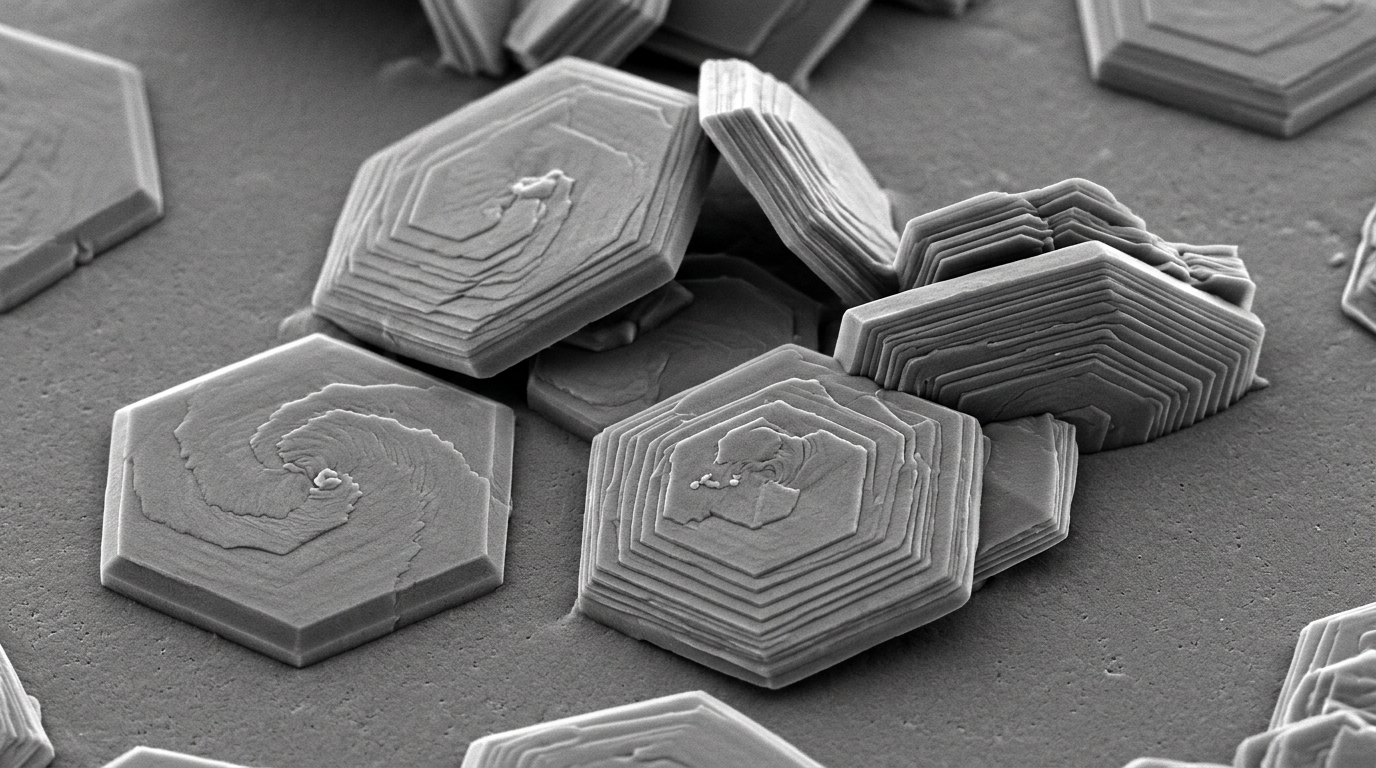
The Williamson-Hall plot yielded a low micro-strain value of 0.08252 for the annealed Bi2Se3 nanoparticles. Because this strain level remained minimal, the researchers concluded that the diffraction peak broadening in the synthesized material was predominantly governed by crystallite size reduction rather than internal lattice deformation. Morphological evaluation using high-resolution scanning electron microscopy (HRSEM) supported the crystalline nature of the powders. The as-prepared material displayed a porous surface texture composed of mixed nanorod and nanoflake structures. In the annealed sample, high-magnification imaging revealed white crystalline selenium nanoparticles well incorporated and dispersed across the bismuth-containing matrix.
Statistical evaluation of the electron micrographs using ImageJ image-processing software showed that the overall particle diameters of the synthesized Bi2Se3 powders were distributed across a size range spanning 20 to 300 nanometers. To probe local vibrational modes and crystal symmetries, micro-Raman spectroscopy was carried out using a 785-nanometer excitation laser source. Rhombohedral Bi2Se3 primitive unit cells contain five atoms arranged in quintuple layers of Se-Bi-Se-Bi-Se bound internally by covalent forces and stacked along the c-axis via weaker van der Waals interactions. Group theory predicts twelve zone-center optical phonon modes, of which four are Raman active: two out-of-plane modes, A11g and A21g, and two in-plane modes, E1g and E2g.
The experimental Raman spectra distinctly exhibited three optical phonon modes located near 124 reciprocal centimeters, 262 reciprocal centimeters, and 524 reciprocal centimeters. The pronounced peak at approximately 124 reciprocal centimeters was assigned to the characteristic E2g lattice vibration, confirming the structural quality of the synthesized crystals. The vibrational band at 262 reciprocal centimeters was attributed to a combination of the A11g and A21g modes reflecting sample crystallinity, while the higher-frequency peak at 524 reciprocal centimeters was identified as originating from overtones of the A11g and E2g modes or stronger localized bonding forces. The lowest-frequency in-plane E1g mode was not resolved, consistent with typical observations where it lies buried near the unshifted Rayleigh excitation line.
Electrochemical properties were evaluated by cyclic voltammetry using a three-electrode configuration comprising a modified glassy carbon working electrode, a platinum wire counter electrode, and a silver/silver chloride reference electrode. Measurements performed in an acetonitrile electrolyte containing tetrabutylammonium perchlorate across potential windows between -0.2 and 1.5 volts exhibited well-defined redox peaks. For the modified glassy carbon electrode bearing annealed Bi2Se3 nanoparticles, cyclic voltammograms recorded at scan rates of 50 to 100 millivolts per second showed enhanced redox current responses, registering an anodic peak current (IPa) of 0.021 microamperes and a cathodic peak current (IPc) of -0.144 microamperes.
This electrochemical response was attributed to the multi-step conversion of trivalent bismuth (Bi3+) ions into divalent bismuth (Bi2+) and metallic bismuth species. Mathematical evaluation of the current response indicated a charge transfer process involving approximately three electrons (calculated value of 3.4), confirming the electroactive redox behavior of the modified surface. Complementary electrical impedance spectroscopy measurements performed on dense cylindrical pellets (0.66 millimeters thick and 0.526 millimeters in diameter) over frequencies from 1 hertz to 1 megahertz and temperatures up to 70 degrees Celsius yielded depressed semicircular Nyquist arcs below the real axis, characteristic of non-Debye relaxation and substantial grain-boundary resistance.
Optical absorption spectra recorded via ultraviolet-visible spectrophotometry across the 220 to 270 nanometer range revealed an absorption maximum centered at 226 nanometers for the as-prepared Bi2Se3 nanoparticles. Tauc plot analysis extrapolating the linear region of (alpha*h*nu)^2 versus photon energy yielded an optical band gap of 3.47 electron volts. This value is significantly wider than the narrow band gap reported for bulk bismuth selenide crystals (0.16 to 0.35 electron volts). The authors noted that this pronounced widening could arise from quantum confinement effects, Moss-Burstein band filling, defect transitions, higher-energy inter-band absorptions, or minor surface oxidation forming bismuth oxide phases during nanoscale synthesis and ambient drying.
Beyond the final voltammetric scans, the experimental protocol incorporated meticulous electrode preparation and surface diagnostic procedures to ensure measurement reproducibility. Before immobilizing the bismuth selenide nanoparticles, the glassy carbon electrode was mechanically polished using an alumina slurry on a polishing cloth moved in a systematic figure-eight motion to eliminate adsorbed surface contaminants. Following abrasive cleaning, the electrode underwent deionized water rinses and ultrasonic agitation in ethanol or water to clear residual alumina particulate debris. The clean working surface was subsequently electrochemically activated through potential cycling in a sulfuric acid solution to establish a stable background baseline current. Surface cleanliness and electron transfer competence were independently verified using a potassium ferricyanide redox test couple prior to material deposition. While the annealed Bi2Se3 modified electrode generated the elevated anodic and cathodic currents noted previously, the as-prepared sample exhibited baseline redox peaks with an anodic peak current of 0.0114 microamperes and a cathodic peak current of -0.155 microamperes in the supporting electrolyte.
The structural and vibrational findings also tied directly to the crystallographic symmetry of the rhombohedral lattice, which belongs to the R-3m space group with measured lattice dimensions of a = 4.1396 angstroms and c = 28.636 angstroms. Within each quintuple-layer unit, atomic layers arrange in an alternating Se1–Bi–Se2–Bi–Se1 stacking sequence along the c-axis, where selenium atoms inhabit two distinct crystallographic sites before terminating at weakly bonded cleavage planes. The authors noted that the observed Raman-active modes reflect clear polarization dependencies governed by specific atomic displacement vectors. When scattering is probed under an x-direction polarization geometry, specifically the z(xx)z configuration, the resulting spectrum displays the out-of-plane A11g and A12g vibrations alongside the in-plane E2g mode. In contrast, evaluating scattered light polarized along the orthogonal y-direction isolates the E2g phonon mode alone, illustrating how directional scattering dynamics govern the visible optical phonon signatures in these layered nanocrystals.
Quantitative electrical evaluation through impedance spectroscopy provided additional details regarding sample conduction and grain-boundary phenomena across variable temperatures up to 70 degrees Celsius. The test geometry positioned the cylindrical Bi2Se3 compact directly between two cylindrical platinum electrodes measuring 0.45 millimeters in thickness and 8 millimeters in diameter. To extract the electrical resistance of the nanocrystalline sample across the applied alternating-current frequencies from 1 hertz to 1 megahertz, the experimental impedance arcs were modeled using a complex non-linear least squares fitting procedure. By taking into account the geometric cross-sectional area and thickness of the pellet, the modeled resistance was directly converted into electrical conductivity through the standard inverse resistivity relation. Minor deviations from ideal semicircular behavior observed at lower frequencies and temperatures further confirmed the presence of non-Debye relaxation mechanisms within the grain structure.
Subject of Research: Solvothermal synthesis and characterization of structural, vibrational, optical, and electrical properties of bismuth selenide nanomaterials
Article Title: A facile synthesis, structural, morphological and electrical properties of Bi2Se3 nanomaterials
Article References: V, A., S, S., G, S., M, P., & K, R. (2026). A facile synthesis, structural, morphological and electrical properties of Bi2Se3 nanomaterials. Journal of Materials Science: Materials in Energy, 2(1), Article 29. https://doi.org/10.1007/s44308-026-00018-1
Image Credits: AI Generated
DOI: 10.1007/s44308-026-00018-1
Keywords: bismuth selenide, nanoparticles, solvothermal synthesis, X-ray diffraction, Raman spectroscopy, cyclic voltammetry, impedance spectroscopy, optical band gap, crystallite size, thermal annealing, nanoflakes, nanorods, glassy carbon electrode, Williamson-Hall analysis, topological insulators, semiconductor nanomaterials
News Source: Denise Maddox. (November 17, 2026). Solvothermal Synthesis Yields Bismuth Selenide Nanoparticles with Distinct Phonon Modes. Scienmag.