


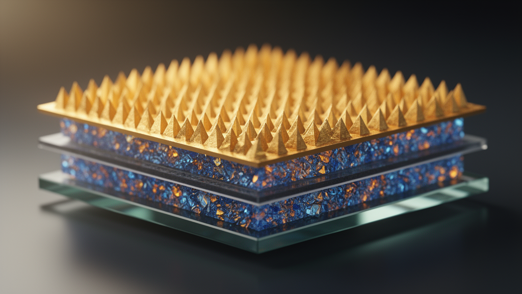
A carefully textured pair of surfaces, one at the front of a solar cell and one buried deep inside it, could squeeze measurably more electricity out of all-perovskite tandem solar cells, according to a simulation study published in Frontiers of Optoelectronics. The work, led by Wenjiang Ye and Aoyue Chen of Huazhong University of Science and Technology together with Ping Fu and colleagues including Jiang Tang and Chao Chen, models what happens when the flat interfaces of a two-terminal perovskite-perovskite tandem device are replaced with periodic, sawtooth-like serrated microstructures. In the simulated devices, the dual serrated design cuts the photocurrent lost to reflection from 4.47 to 3.65 milliamperes per square centimeter, an 18.34 percent reduction, and is expected to lift power conversion efficiency to approximately 31.13 percent, a 3.41 percent increase over the flat baseline.
All-perovskite tandem solar cells stack two light-absorbing perovskite layers with different bandgaps: a wide-bandgap top cell that soaks up high-energy visible photons and a narrow-bandgap bottom cell that captures the redder and near-infrared light that passes through. Because the two subcells are wired in series, the current flowing through the whole device is limited by whichever subcell produces less of it, so balancing the photocurrents is a central design constraint. Real devices of this class have already reached a power conversion efficiency of 30.1 percent, yet the authors note that the theoretical maximum for the technology stands near 45 percent. The gap between those two numbers is largely optical: photons that are reflected away, absorbed parasitically by non-active layers, or otherwise never converted into charge carriers represent energy that no circuit trick can recover.
The scale of that problem is what motivated the new study. For a specific structure of all-perovskite tandem cell, previous analysis cited in the paper indicates that optical losses account for roughly 31.15 percent of total energy loss, and that reflection alone contributes as much as 19.64 percent of that loss. In the team’s own optical model of the highest-efficiency all-perovskite tandem structure reported to date, reflection losses consumed 10.84 percent of the total photocurrent density, equivalent to 4.47 milliamperes per square centimeter. Spectral analysis of the flat reference device revealed prominent reflection peaks exceeding 20 percent at several wavelengths, including 350, 550, 750 and 950 nanometers, which the authors attribute to refractive index mismatch at the front interface that bounces incident light away instead of coupling it into the perovskite absorbers.
To quantify these effects, the researchers built an optical model in COMSOL Multiphysics, solving Maxwell’s equations with Floquet-Bloch boundary conditions and perfectly matched layers to compute absorption, reflection and transmission across the device stack. From the spatial and spectral distribution of photogenerated carriers, they integrated the photocurrent density produced separately in the wide-bandgap and narrow-bandgap layers. The modeled device used a wide-bandgap perovskite with a bandgap of 1.8 electronvolts and a narrow-bandgap perovskite at 1.25 electronvolts, with thickness scans identifying 400 nanometers and 1200 nanometers as the optimal layer thicknesses. In the flat baseline, the two subcells generated nearly balanced photocurrents of 16.42 and 16.50 milliamperes per square centimeter respectively, a configuration consistent with the literature on the record-setting device architecture.
The first round of optimization targeted the front interface, where sunlight enters the stack. The team added a periodic serrated texture with a fixed period of 1 micrometer and varied its height from 300 to 1000 nanometers. The texture behaves something like an array of microscopic lenses: in the 400 to 700 nanometer absorption range of the wide-bandgap subcell, it focuses light and boosts the electric field intensity at the front interface to a simulated maximum of 100 volts per meter, four times the value in the flat structure. At a wavelength of 1000 nanometers, the serrations disrupt the waveguide modes that persist in the flat device and raise the maximum electric field in the narrow-bandgap layer to 70 volts per meter, a 1.5-fold increase. With the front serration height set to 400 nanometers, reflection in the 300 to 700 nanometer band dropped by about 5 percent and reflection in the 700 to 1000 nanometer band fell by roughly 10 percent, cutting the reflection-loss current density from 4.47 to 3.77 milliamperes per square centimeter, a 15.66 percent reduction, and pushing the tandem photocurrent to a peak of 16.84 milliamperes per square centimeter, a 2.56 percent gain.
Yet the front texture alone could not fix everything. Around 950 nanometers, deep in the narrow-bandgap cell’s territory, roughly 20 percent of the light was still being reflected, and because the tandem’s current is capped by the weaker subcell, that residual loss limited further gains. The authors also observed a trade-off: once the front serration height exceeded 400 nanometers, reflection in the short-wavelength band kept improving, but reflection near 1000 nanometers began to climb, canceling out the benefit. So the team turned to the other end of the device, designing the same periodic serrated structure on the back electrode, a geometry that could in practice be realized by nanoimprinting the perovskite layer and then depositing the metal cathode.
The back serrations work by a different optical mechanism. In the long-wavelength absorption range of the narrow-bandgap subcell, from 700 to 1000 nanometers, the textured back electrode promotes photon cycling, bouncing weakly absorbed infrared light back through the absorber repeatedly. The simulated maximum electric field in the narrow-bandgap layer rose to 80 volts per meter, nearly 1.7 times the uniformly decaying field seen in the flat structure. The authors also report that infrared light excites surface plasmon polaritons at the serrated tips of the silver-narrow-bandgap interface, near-field effects that further improve the layer’s ability to absorb long-wavelength light. With the back serration height at 400 nanometers, reflection in the 700 to 1000 nanometer range decreased by about 5 percent, the reflection-loss current fell from 4.47 to 4.10 milliamperes per square centimeter, an 8.28 percent reduction, and the narrow-bandgap subcell’s photocurrent rose to 16.93 milliamperes per square centimeter, a 2.61 percent improvement. Because the wide-bandgap subcell was untouched and still produced 16.42 milliamperes per square centimeter, the tandem current remained pinned at that value.
The full benefit emerged only when the two textures were combined. Scanning the front height H1 and back height H2 jointly, the team found an optimum at 550 nanometers for the front serrations and 400 nanometers for the back serrations, yielding a maximum tandem photocurrent density of 16.98 milliamperes per square centimeter. In this dual-textured configuration, the front structure continues to focus short-wavelength light into the wide-bandgap absorber, where the maximum electric field reaches 100 volts per meter, four times the flat value, while the back structure scatters and traps long-wavelength light, doubling the maximum electric field in the narrow-bandgap layer to 100 volts per meter at 1000 nanometers. The combined design cut the reflection-induced photocurrent loss to 3.65 milliamperes per square centimeter, the 18.34 percent reduction, and the authors expect it to raise device efficiency to approximately 31.13 percent, a 3.41 percent increase relative to the flat structure.
It is important to read these numbers for what they are: results of an optical simulation, not measurements from a fabricated cell. The study models how light propagates, scatters and is absorbed in an idealized device stack; it does not demonstrate that serrated perovskite layers can be manufactured with the required precision, that the textured interfaces would preserve the electrical quality of the junctions, or that the predicted efficiency would survive real-world defects, degradation and processing variability. The authors themselves frame the work as providing a theoretical foundation and design strategies, and they note that future research will focus on further minimizing residual reflection losses while maintaining current matching between the two subcells. The data supporting the study are available from the corresponding author upon reasonable request.
Even with those caveats, the findings land at a consequential moment for perovskite photovoltaics. Tandem architectures are widely viewed as the most credible route to push solar conversion efficiencies beyond the limits of single-junction cells, and all-perovskite tandems promise to deliver that leap without the cost and complexity of crystalline silicon bottom cells. Earlier attempts to tame reflection in these devices have included embedding micrometer-sized resin particles in the narrow-bandgap layer, which boosted infrared absorption by about 10 percent, tuning absorber thicknesses to balance the two subcells, and coating glass with fluorine-doped tin oxide nanoplates that cut reflection across the spectrum by roughly 5 percent. The dual serrated approach adds a complementary lever: geometry applied at both the entry and exit of the light’s journey through the stack, tuned so that each texture addresses the spectral band where it does the most good. If experimental groups can translate the simulated sawtooth profiles into working devices, the modeled 31.13 percent efficiency suggests that a significant slice of the enormous gap between today’s 30.1 percent and the 45 percent theoretical ceiling may be recoverable simply by reshaping the surfaces the light encounters on its way through the cell.
Subject of Research: Optical simulation of dual serrated microstructures for reducing reflection losses in all-perovskite tandem solar cells
Article Title: Simulation study of reducing reflection losses in all-perovskite tandem solar cells through dual serrated structure
Article References: Ye, W., Chen, A., Fu, P., Tang, J., & Chen, C. (2025). Simulation study of reducing reflection losses in all-perovskite tandem solar cells through dual serrated structure. Frontiers of Optoelectronics, 18(1), Article 9. https://doi.org/10.1007/s12200-025-00153-7
Image Credits: AI Generated
DOI: 10.1007/s12200-025-00153-7
Keywords: perovskite, tandem solar cells, reflection losses, light trapping, serrated structure, photovoltaics, optical simulation, COMSOL, power conversion efficiency, photon cycling, surface plasmon polaritons, current matching
News Source: Denise Maddox. (October 30, 2026). Serrated Surfaces Could Push All-Perovskite Tandem Solar Cells Toward 31 Percent Efficiency in Simulations. Scienmag.