


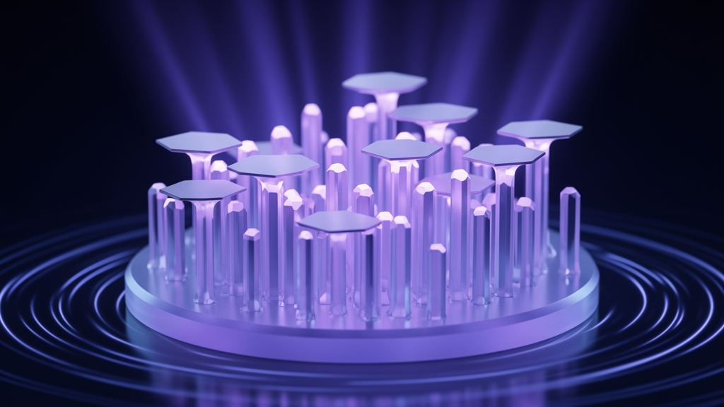
A self-powered ultraviolet photodetector built from a GaN nanopillar and a transparent graphene top contact has been designed and simulated in detail, and the numbers coming out of the model are striking. Operating with no external bias at all, the simulated device produces a photocurrent of 3.92 microamperes at a wavelength of 280 nanometres under 10 microwatts of illumination, a responsivity of 0.07714 amperes per watt once the geometry of the nanopillar array is accounted for, and a rise time of just 7.7 nanoseconds. Even so, the design offers a concrete blueprint for a class of detectors that could matter enormously in ultraviolet optical wireless communication, where short-range, solar-blind links are needed without the burden of a power supply.
The appeal of self-powered photodetection lies in physics rather than electronics. Conventional ultraviolet detectors generally need an external bias to separate the electron-hole pairs that light creates, which adds energy consumption, dark current and system complexity. A self-powered device instead works in photovoltaic mode: a built-in electric field inside the junction does the separating, sweeping electrons one way and holes the other, generating a photocurrent with no applied voltage. That makes such detectors attractive for remote or energy-constrained settings, from underwater sensing to space applications, and it removes a whole layer of hardware from any communication system built around them.
The material at the heart of the design is gallium nitride, a wide-bandgap semiconductor with a direct bandgap of 3.44 electronvolts. That gap makes GaN naturally blind to visible light, so a GaN detector ignores sunlight and responds only to ultraviolet photons, a property that dramatically improves signal-to-noise ratios in outdoor environments. GaN also brings a thermal conductivity of 2.1 watts per centimetre-kelvin, strong chemical stability, radiation hardness, an electron mobility near 900 square centimetres per volt-second, and a breakdown field of roughly 3.3 megavolts per centimetre, all of which support fast, sensitive and durable photodetection in harsh conditions.
Geometry matters as much as material. The proposed device is a vertical p-i-n structure, with a 50-nanometre p-type GaN cap, a 300-nanometre intrinsic region shaped into a nanopillar of 100-nanometre diameter, and a 150-nanometre n-type base, all sitting under a 1.5-nanometre tri-layer graphene sheet and on top of a 5-nanometre aluminium contact. Shrinking GaN to these lateral dimensions relaxes lattice strain, reduces structural defects and raises the surface-to-volume ratio, which enhances photon absorption through light trapping and optical confinement. The nanopillar array is arranged on a square grid with a 200-nanometre pitch, giving a geometric fill factor of 19.63 percent, a number that turns out to be crucial for interpreting the device’s responsivity.
The asymmetric contact scheme is the design’s most distinctive feature. Graphene, with a work function of 4.6 electronvolts for a tri-layer sheet, forms a Schottky contact on p-type GaN, while aluminium, with a work function of 4.26 electronvolts, forms a near-ohmic contact on the n-type side, with an estimated electron barrier of only about 0.16 electronvolts. Symmetric electrode pairs, by contrast, produce zero net contact potential difference and rely entirely on the doping profile, which the simulations show yields no current at zero bias. The graphene-aluminium mismatch adds a unidirectional electrostatic field that reinforces the p-i-n built-in field, and the graphene/p-GaN Schottky junction generates an intense localised field spike of about 4.5 by ten-to-the-six volts per metre that accelerates hole extraction, while the wide intrinsic region sustains a uniform plateau field of roughly 1.79 by ten-to-the-six volts per metre.
Because graphene is nearly transparent, the top electrode lets most ultraviolet photons through to the active region instead of absorbing them, as an opaque metal would. The tri-layer choice is a deliberate compromise: thicker few-layer graphene reaches the higher work function needed for an effective Schottky barrier with p-GaN, while the 1.5-nanometre thickness keeps optical attenuation minimal. The simulations also included realistic imperfections, a finite graphene sheet resistance and a specific contact resistivity of 1.3 by ten-to-the-minus-three ohm-square centimetres at the graphene/GaN interface, plus trap-assisted surface recombination, so the modelled dark current reflects non-ideal transport rather than a perfect contact.
The optical results show the device absorbing most strongly at 260 nanometres, with strong absorption maintained from 200 to 290 nanometres, covering deep UV-C and UV-B. Reflectance is very low between 250 and 300 nanometres, meaning incident light is converted into carriers rather than bounced away, and absorption falls sharply beyond 320 nanometres, confirming visible-blind operation. Under illumination, the simulated photocurrent peaks at 3.92 microamperes at 280 nanometres. Dividing by the incident power gives 0.392 amperes per watt before geometry is considered; scaling by the 19.63 percent fill factor yields the effective responsivity of 0.07714 amperes per watt, corresponding to an external quantum efficiency of about 34.16 percent at 280 nanometres, achieved entirely at zero bias.
The dark-side numbers are equally important for sensing. With the optical generation rate set to zero, the simulated dark current is an extremely low 1.309 by ten-to-the-elevenths of an ampere, suppressed by GaN’s wide bandgap and the broad depletion region of the p-i-n structure. That produces a photo-to-dark-current ratio of 2.99 by ten-to-the-fifth, a noise current of 2.048 by ten-to-the-fifteenths amperes per root-hertz, a noise-equivalent power of 2.6597 by ten-to-the-fourteenths watts per root-hertz, and a specific detectivity of 3.3113 by ten-to-the-thirteenth Jones at 280 nanometres. The authors caution that in a real fabricated device, interface states, transfer residues and surface contamination could raise leakage, so interface passivation and optimised graphene transfer would likely be needed to approach the simulated performance.
Speed and bandwidth tell a two-part story. An equivalent RC analysis, using a simulated resistance of 0.0092336 ohms and capacitance of 1.1154 by ten-to-the-twelfth farads, gives a theoretical RC-limited bandwidth of about 15.4 terahertz, an upper limit the authors explicitly interpret as such rather than an achievable system figure, since probe pads, interconnects, load resistance and trap-related slow processes would all cut into it in practice. The more realistic operational bandwidth comes from the transient response: with simulated rise and fall times of 7.7 and 8.6 nanoseconds, the standard relation linking fall time to bandwidth yields about 40.7 megahertz. The slightly longer fall time than rise time points to carrier trapping and residual charge release from localised states, effects that could worsen without good surface passivation.
To test what those device numbers would mean in a communication link, the team ran a MATLAB system-level simulation using non-return-to-zero on-off keying at 50 megabits per second, with a beam divergence of 10 degrees and atmospheric extinction of 1.2 by ten-to-the-minus-three per metre at 280 nanometres. The signal-to-noise ratio falls from about 62 decibels at one metre to about 5.5 decibels at 25 metres, and the bit-error rate stays below ten-to-the-minus-fifth out to 11.5 metres, reaching the forward-error-correction threshold of 3.8 by ten-to-the-minus-third at 14.5 metres. Within the model’s assumptions, the detector’s 40.7-megahertz bandwidth supports stable short-range ultraviolet wireless links without any external bias. The study also explored thickness optimisation, finding responsivity rising from 0.023 to 0.138 amperes per watt as the active layer grows from 100 to 1000 nanometres before recombination losses take over beyond 5 micrometres, and a contact comparison showing that although nickel and platinum form stronger Schottky barriers, graphene offers the best balance of barrier height, carrier extraction and optical transparency. As a simulation study, the work establishes a design target rather than a demonstrated device, but it maps a plausible route toward zero-power ultraviolet receivers for short-range optical wireless networks.
Subject of Research: Computational design and COMSOL simulation of a graphene/GaN nanopillar self-powered ultraviolet photodetector for optical wireless communication
Article Title: Device design & simulation of a graphene/ p-GaN/ i-GaN-nanopillar /n-GaN, self-powered UV photodetectors toward wireless communication
Article References: Jebas, E. P., & Palla, P. (2026). Device design & simulation of a graphene/ p-GaN/ i-GaN-nanopillar /n-GaN, self-powered UV photodetectors toward wireless communication. Results in Optics, Article 101199. https://doi.org/10.1016/j.rio.2026.101199
Image Credits: AI Generated
DOI: 10.1016/j.rio.2026.101199
Keywords: GaN, graphene, self-powered photodetector, ultraviolet detection, optical wireless communication, p-i-n junction, Schottky contact, nanopillar, COMSOL simulation, dark current, responsivity, solar-blind
News Source: Neil Sanderson. (October 29, 2026). Simulated Graphene-GaN Nanopillar Photodetector Runs on Zero Power for UV Wireless Links. Scienmag.